
Datasheet

STM32F103x4, STM32F103x6 Package characteristics
Doc ID 15060 Rev 6 77/90
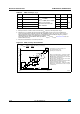
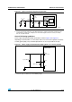
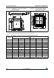
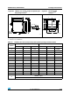
Figure 40. UFQFPN48 7 x 7 mm, 0.5 mm pitch, package outline
1. Drawing is not to scale.
2. There is an exposed die pad on the underside of the QFPN package, this pad is not internally connected to
the VSS or VDD power pads. It is recommended to connect it to VSS.
3. All leads/pads should also be soldered to the PCB to improve the lead solder joint life.
!"?-%?6
$
0ININDENTIFIER
LASERMARKINGAREA
%%
$
9
$
%
%XPOSEDPAD
AREA
:
$ETAIL:
2TYP
,
#X
PINCORNER
!
3EATING
PLANE
!
B
E
DDD
$ETAIL9
4
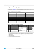
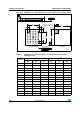
Table 52. UFQFPN48 7 x 7 mm, 0.5 mm pitch, package mechanical data
Symbol
millimeters inches
(1)
Min Typ Max Min Typ Max
A 0.500 0.550 0.600 0.0197 0.0217 0.0236
A1 0.000 0.020 0.050 0.0000 0.0008 0.0020
D 6.900 7.000 7.100 0.2717 0.2756 0.2795
E 6.900 7.000 7.100 0.2717 0.2756 0.2795
L 0.300 0.400 0.500 0.0118 0.0157 0.0197
T 0.152 0.0060
b 0.200 0.250 0.300 0.0079 0.0098 0.0118
e 0.500 0.0197
ddd 0.080 0.0031