
Datasheet

STM32F103x4, STM32F103x6 Electrical characteristics
Doc ID 15060 Rev 6 73/90
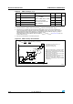
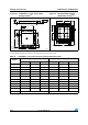
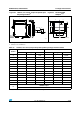
Figure 35. Typical connection diagram using the ADC
1. Refer to Ta bl e 46 for the values of R
AIN
, R
ADC
and C
ADC
.
2. C
parasitic
represents the capacitance of the PCB (dependent on soldering and PCB layout quality) plus the
pad capacitance (roughly 7 pF). A high C
parasitic
value will downgrade conversion accuracy. To remedy
this, f
ADC
should be reduced.
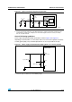
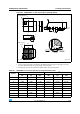
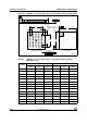
General PCB design guidelines
Power supply decoupling should be performed as shown inFigure 36 or Figure 37,
depending on whether V
REF+
is connected to V
DDA
or not. The 10 nF capacitors should be
ceramic (good quality). They should be placed them as close as possible to the chip.
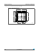
Figure 36. Power supply and reference decoupling (V
REF+
not connected to V
DDA
)
1. The V
REF+
input is available only on the TFBGA64 package.
ai14150c
STM32F103xx
V
DD
AINx
I
L
±1 µA
0.6 V
V
T
R
AIN
(1)
C
parasitic
V
AIN
0.6 V
V
T
R
ADC
(1)
12-bit
converter
C
ADC
(1)
Sample and hold ADC
converter
6
2%&
SEENOTE
34-&XX
6
$$!
6
33!
&N&
&N&
AI