
Datasheet

STM32F103x4, STM32F103x6 Electrical characteristics
Doc ID 15060 Rev 6 71/90
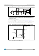
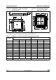
Equation 1: R
AIN
max formula:
The formula above (Equation 1) is used to determine the maximum external impedance allowed for an
error below 1/4 of LSB. Here N = 12 (from 12-bit resolution).
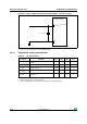
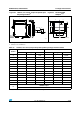
Table 47. R
AIN
max for f
ADC
= 14 MHz
(1)
1. Based on characterization, not tested in production.
T
s
(cycles) t
S
(µs) R
AIN
max (kΩ)
1.5 0.11 0.4
7.5 0.54 5.9
13.5 0.96 11.4
28.5 2.04 25.2
41.5 2.96 37.2
55.5 3.96 50
71.5 5.11 NA
239.5 17.1 NA
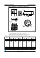
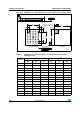
Table 48. ADC accuracy - limited test conditions
(1)
(2)
1. ADC DC accuracy values are measured after internal calibration.
2. ADC Accuracy vs. Negative Injection Current: Injecting a negative current on any analog input pins should
be avoided as this significantly reduces the accuracy of the conversion being performed on another analog
input. It is recommended to add a Schottky diode (pin to ground) to analog pins which may potentially inject
negative currents.
Any positive injection current within the limits specified for I
INJ(PIN)
and ΣI
INJ(PIN)
in Section 5.3.12 does not
affect the ADC accuracy.
Symbol Parameter Test conditions Typ Max
(3)
3. Based on characterization, not tested in production.
Unit
ET Total unadjusted error
f
PCLK2
= 56 MHz,
f
ADC
= 14 MHz, R
AIN
< 10 kΩ,
V
DDA
= 3 V to 3.6 V
T
A
= 25 °C
Measurements made after
ADC calibration
±1.3 ±2
LSB
EO Offset error ±1 ±1.5
EG Gain error ±0.5 ±1.5
ED Differential linearity error ±0.7 ±1
EL Integral linearity error ±0.8 ±1.5
R
AIN
T
S
f
ADC
C
ADC
2
N2+
()ln××
--------------------------------------------------------------- - R
ADC
–<