
Datasheet


STM32F103x4, STM32F103x6 Electrical characteristics
Doc ID 15060 Rev 6 61/90
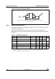
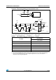
Input/output AC characteristics
The definition and values of input/output AC characteristics are given in Figure 27 and
Tabl e 37 , respectively.
Unless otherwise specified, the parameters given in Ta ble 3 7 are derived from tests
performed under the ambient temperature and V
DD
supply voltage conditions summarized
in Ta bl e 9 .
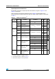
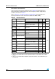
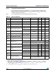
Table 37. I/O AC characteristics
(1)
1. The I/O speed is configured using the MODEx[1:0] bits. Refer to the STM32F10xxx reference manual for a
description of GPIO Port configuration register.
MODEx[1:0]
bit value
(1)
Symbol Parameter Conditions Min Max Unit
10
f
max(IO)out
Maximum frequency
(2)
2. The maximum frequency is defined in Figure 27.
C
L
= 50 pF, V
DD
= 2 V to 3.6 V 2 MHz
t
f(IO)out
Output high to low
level fall time
C
L
= 50 pF, V
DD
= 2 V to 3.6 V
125
(3)
3. Guaranteed by design, not tested in production.
ns
t
r(IO)out
Output low to high
level rise time
125
(3)
01
f
max(IO)out
Maximum frequency
(2)
C
L
= 50 pF, V
DD
= 2 V to 3.6 V 10 MHz
t
f(IO)out
Output high to low
level fall time
C
L
= 50 pF, V
DD
= 2 V to 3.6 V
25
(3)
ns
t
r(IO)out
Output low to high
level rise time
25
(3)
11
F
max(IO)out
Maximum frequency
(2)
C
L
= 30 pF, V
DD
= 2.7 V to 3.6 V 50 MHz
C
L
= 50 pF, V
DD
= 2.7 V to 3.6 V 30 MHz
C
L
= 50 pF, V
DD
= 2 V to 2.7 V 20 MHz
t
f(IO)out
Output high to low
level fall time
C
L
= 30 pF, V
DD
= 2.7 V to 3.6 V 5
(3)
ns
C
L
= 50 pF, V
DD
= 2.7 V to 3.6 V 8
(3)
C
L
= 50 pF, V
DD
= 2 V to 2.7 V 12
(3)
t
r(IO)out
Output low to high
level rise time
C
L
= 30 pF, V
DD
= 2.7 V to 3.6 V 5
(3)
C
L
= 50 pF, V
DD
= 2.7 V to 3.6 V 8
(3)
C
L
= 50 pF, V
DD
= 2 V to 2.7 V 12
(3)
-t
EXTIpw
Pulse width of
external signals
detected by the EXTI
controller
10 ns