
Datasheet

Electrical characteristics STM32F103x4, STM32F103x6
60/90 Doc ID 15060 Rev 6
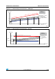
Output driving current
The GPIOs (general-purpose inputs/outputs) can sink or source up to ±8 mA, and sink or
source up to ±20 mA (with a relaxed V
OL
/V
OH
) except PC13, PC14 and PC15 which can
sink or source up to +/-3mA. When using the GPIOs PC13 to PC15 in output mode, the
speed should not exceed 2 MHz with a maximum load of 30 pF.
In the user application, the number of I/O pins which can drive current must be limited to
respect the absolute maximum rating specified in Section 5.2:
● The sum of the currents sourced by all the I/Os on V
DD,
plus the maximum Run
consumption of the MCU sourced on V
DD,
cannot exceed the absolute maximum rating
I
VDD
(see Ta bl e 7).
● The sum of the currents sunk by all the I/Os on V
SS
plus the maximum Run
consumption of the MCU sunk on V
SS
cannot exceed the absolute maximum rating
I
VSS
(see Ta bl e 7 ).
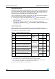
Output voltage levels
Unless otherwise specified, the parameters given in Ta ble 3 6 are derived from tests
performed under ambient temperature and V
DD
supply voltage conditions summarized in
Tabl e 9. All I/Os are CMOS and TTL compliant.
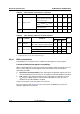
Table 36. Output voltage characteristics
Symbol Parameter Conditions Min Max Unit
V
OL
(1)
1. The I
IO
current sunk by the device must always respect the absolute maximum rating specified in Table 7
and the sum of I
IO
(I/O ports and control pins) must not exceed I
VSS
.
Output low level voltage for an I/O pin
when 8 pins are sunk at same time
CMOS port
(2)
,
I
IO
= +8 mA
2.7 V < V
DD
< 3.6 V
2. TTL and CMOS outputs are compatible with JEDEC standards JESD36 and JESD52.
0.4
V
V
OH
(3)
3. The I
IO
current sourced by the device must always respect the absolute maximum rating specified in
Table 7 and the sum of I
IO
(I/O ports and control pins) must not exceed I
VDD
.
Output high level voltage for an I/O pin
when 8 pins are sourced at same time
V
DD
–0.4
V
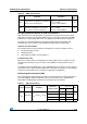
OL
(1)
Output low level voltage for an I/O pin
when 8 pins are sunk at same time
TTL port
(2)
I
IO
=+ 8mA
2.7 V < V
DD
< 3.6 V
0.4
V
V
OH
(3)
Output high level voltage for an I/O pin
when 8 pins are sourced at same time
2.4
V
OL
(1)(4)
4. Based on characterization data, not tested in production.
Output low level voltage for an I/O pin
when 8 pins are sunk at same time
I
IO
= +20 mA
2.7 V < V
DD
< 3.6 V
1.3
V
V
OH
(3)(4)
Output high level voltage for an I/O pin
when 8 pins are sourced at same time
V
DD
–1.3
V
OL
(1)(4)
Output low level voltage for an I/O pin
when 8 pins are sunk at same time
I
IO
= +6 mA
2 V < V
DD
< 2.7 V
0.4
V
V
OH
(3)(4)
Output high level voltage for an I/O pin
when 8 pins are sourced at same time
V
DD
–0.4