
Datasheet

Electrical characteristics STM32F103x4, STM32F103x6
56/90 Doc ID 15060 Rev 6
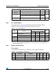
5.3.13 I/O port characteristics
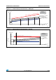
General input/output characteristics
Unless otherwise specified, the parameters given in Ta ble 3 5 are derived from tests
performed under the conditions summarized in Tabl e 9. All I/Os are CMOS and TTL
compliant.
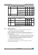
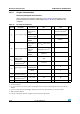
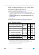
Table 35. I/O static characteristics
Symbol Parameter Conditions Min Typ Max Unit
V
IL
Low level input voltage
Standard IO
input low level
voltage
- - 0.28*(V
DD
-2 V)+0.8 V
(1)
V
IO FT
(3)
input
low level voltage
- - 0.32*(V
DD
-2V)+0.75 V
(1)
All I/Os except
BOOT0
- - 0.35V
DD
(2)
V
IH
High level input voltage
Standard IO
input high level
voltage
0.41*(V
DD
-2 V)+1.3 V
(1)
--
IO FT
(3)
input
high level
voltage
0.42*(V
DD
-2 V)+1 V
(1)
--
All I/Os except
BOOT0
0.65V
DD
(2)
--
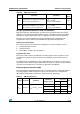
V
hys
Standard IO Schmitt
trigger voltage
hysteresis
(4)
200 - -
mV
IO FT Schmitt trigger
voltage hysteresis
(4)
5% V
DD
(5)
--
I
lkg
Input leakage current
(6)
V
SS
≤ V
IN
≤ V
DD
Standard I/Os
--±1
µA
V
IN
= 5 V
I/O FT
--3
R
PU
Weak pull-up
equivalent resistor
(7)
V
IN
= V
SS
30 40 50
kΩ
R
PD
Weak pull-down
equivalent resistor
(7)
V
IN
= V
DD
30 40 50
C
IO
I/O pin capacitance - 5 - pF
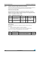
1. Data based on design simulation.
2. Tested in production.
3. FT = Five-volt tolerant. In order to sustain a voltage higher than V
DD
+0.3 the internal pull-up/pull-down resistors must be
disabled.
4. Hysteresis voltage between Schmitt trigger switching levels. Based on characterization, not tested in production.
5. With a minimum of 100 mV.
6. Leakage could be higher than max. if negative current is injected on adjacent pins.