
Datasheet

STM32F103x4, STM32F103x6 Electrical characteristics
Doc ID 15060 Rev 6 51/90
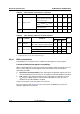
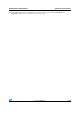
5.3.8 PLL characteristics
The parameters given in Ta ble 2 7 are derived from tests performed under ambient
temperature and V
DD
supply voltage conditions summarized in Tabl e 9.
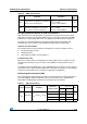
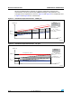
5.3.9 Memory characteristics
Flash memory
The characteristics are given at T
A
= –40 to 105 °C unless otherwise specified.
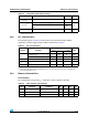
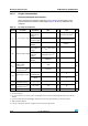
Table 26. Low-power mode wakeup timings
Symbol Parameter Typ Unit
t
WUSLEEP
(1)
1. The wakeup times are measured from the wakeup event to the point in which the user application code
reads the first instruction.
Wakeup from Sleep mode 1.8 µs
t
WUSTOP
(1)
Wakeup from Stop mode (regulator in run mode) 3.6
µs
Wakeup from Stop mode (regulator in low power
mode)
5.4
t
WUSTDBY
(1)
Wakeup from Standby mode 50 µs
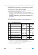
Table 27. PLL characteristics
Symbol Parameter
Value
Unit
Min
(1)
1. Based on characterization, not tested in production.
Typ Max
(1)
f
PLL_IN
PLL input clock
(2)
2. Take care of using the appropriate multiplier factors so as to have PLL input clock values compatible with
the range defined by f
PLL_OUT
.
18.0 25 MHz
PLL input clock duty cycle 40 60 %
f
PLL_OUT
PLL multiplier output clock 16 72 MHz
t
LOCK
PLL lock time 200 µs
Jitter Cycle-to-cycle jitter 300 ps
Table 28. Flash memory characteristics
Symbol Parameter Conditions Min
(1)
Typ Max
(1)
Unit
t
prog
16-bit programming time T
A
= –40 to +105 °C 40 52.5 70 µs
t
ERASE
Page (1 KB) erase time T
A
= –40 to +105 °C 20 40 ms
t
ME
Mass erase time T
A
= –40 to +105 °C 20 40 ms