
Datasheet

STM32F103x4, STM32F103x6 Electrical characteristics
Doc ID 15060 Rev 6 33/90
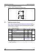
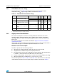
5.3.2 Operating conditions at power-up / power-down
Subject to general operating conditions for T
A
.
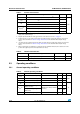
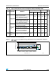
Table 10. Operating conditions at power-up / power-down
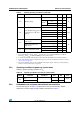
5.3.3 Embedded reset and power control block characteristics
The parameters given in Ta ble 1 1 are derived from tests performed under ambient
temperature and V
DD
supply voltage conditions summarized in Tabl e 9.
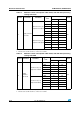
V
IN
I/O input voltage
Standard IO –0.3
V
DD
+
0.3
V
FT IO
(3)
2 V < V
DD
≤ 3.6 V –0.3 5.5
V
DD
= 2 V –0.3 5.2
BOOT0 0 5.5
P
D
Power dissipation at T
A
= 85 °C
for suffix 6 or T
A
= 105 °C for
suffix 7
(4)
TFBGA64 308
mW
LQFP64 444
LQFP48 363
UFQFPN48 624
VFQFPN36 1000
T
A
Ambient temperature for 6
suffix version
Maximum power dissipation –40 85
°C
Low power dissipation
(5)
–40 105
Ambient temperature for 7
suffix version
Maximum power dissipation –40 105
Low power dissipation
(5)
–40 125
T
J Junction temperature range
6 suffix version –40 105
7 suffix version –40 125
1. When the ADC is used, refer to Table 46: ADC characteristics.
2. It is recommended to power V
DD
and V
DDA
from the same source. A maximum difference of 300 mV
between V
DD
and V
DDA
can be tolerated during power-up and operation.
3. To sustain a voltage higher than V
DD
+0.3 V, the internal pull-up/pull-down resistors must be disabled.
4. If T
A
is lower, higher P
D
values are allowed as long as T
J
does not exceed T
J
max (see Table 6.2: Thermal
characteristics on page 83).
5. In low power dissipation state, T
A
can be extended to this range as long as T
J
does not exceed T
J
max (see
Table 6.2: Thermal characteristics on page 83).
Table 9. General operating conditions (continued)
Symbol Parameter Conditions Min Max Unit
Symbol Parameter Conditions Min Max Unit
t
VDD
V
DD
rise time rate 0 ∞
µs/V
V
DD
fall time rate 20 ∞