
Datasheet


STM32F103x4, STM32F103x6 Electrical characteristics
Doc ID 15060 Rev 6 63/90
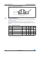
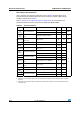
Figure 28. Recommended NRST pin protection
2. The reset network protects the device against parasitic resets.
3. The user must ensure that the level on the NRST pin can go below the V
IL(NRST)
max level specified in
Table 38. Otherwise the reset will not be taken into account by the device.
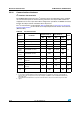
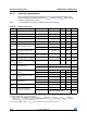
5.3.15 TIM timer characteristics
The parameters given in Ta ble 3 9 are guaranteed by design.
Refer to Section 5.3.12: I/O current injection characteristics for details on the input/output
alternate function characteristics (output compare, input capture, external clock, PWM
output).
ai14132d
STM32F10x
R
PU
NRST
(2)
V
DD
Filter
Internal reset
0.1 µF
External
reset circuit
(1)
Table 39. TIMx
(1)
characteristics
1. TIMx is used as a general term to refer to the TIM1, TIM2, TIM3 and TIM4 timers.
Symbol Parameter Conditions Min Max Unit
t
res(TIM)
Timer resolution time
1
t
TIMxCLK
f
TIMxCLK
= 72 MHz
13.9 ns
f
EXT
Timer external clock
frequency on CH1 to CH4
0
f
TIMxCLK
/2
MHz
f
TIMxCLK
= 72 MHz
036MHz
Res
TIM
Timer resolution 16 bit
t
COUNTER
16-bit counter clock period
when internal clock is
selected
1 65536
t
TIMxCLK
f
TIMxCLK
= 72 MHz
0.0139 910 µs
t
MAX_COUNT
Maximum possible count
65536 × 65536
t
TIMxCLK
f
TIMxCLK
= 72 MHz
59.6 s