
Datasheet


Electrical characteristics STM32F102x8, STM32F102xB
68/80 DocID15056 Rev 5
Figure 31. ADC accuracy characteristics
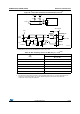
Figure 32. Typical connection diagram using the ADC
1. Refer to Table 47 for the values of R
AIN
, R
ADC
and C
ADC
.
2. C
parasitic
represents the capacitance of the PCB (dependent on soldering and PCB layout quality) plus the
pad capacitance (roughly 7 pF). A high C
parasitic
value will downgrade conversion accuracy. To remedy
this, f
ADC
should be reduced.
E
O
E
G
1LSB
IDEAL
(1) Example of an actual transfer curve
(2) The ideal transfer curve
(3) End point correlation line
E
T
=Total u nadjusted er ror: maximum deviation
between the actual and the ideal transfer curves.
E
O
=Offset error: deviation between the first actual
transition and the first ideal one.
E
G
=Gain er ror: deviation between the last ideal
transition and the last actual one.
E
D
=Differential linearity error: maximum deviation
between actual steps and the ideal one.
E
L
=Integral linearity error: maximum deviation
between any actual transition and the end point
correlation line.
4095
4094
4093
5
4
3
2
1
0
7
6
1234567
4093 4094 4095 4096
(1)
(2)
E
T
E
D
E
L
(3)
V
DDA
V
SSA
ai15497
V
DDA
4096
[1LSB
IDEAL
=
ai14974b
STM32F102
V
DD
AINx
I
L
±1 µA
0.6 V
V
T
R
AIN
(1)
C
parasitic
V
AIN
0.6 V
V
T
R
ADC
(1)
12-bit
converter
C
ADC
(1)
Sample and hold ADC
converter