
Datasheet


Electrical characteristics STM32F102x8, STM32F102xB
54/80 DocID15056 Rev 5
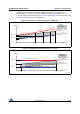
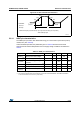
Figure 22. 5 V tolerant I/O input characteristics - CMOS port
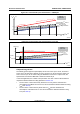
Figure 23. 5 V tolerant I/O input characteristics - TTL port
Output driving current
The GPIOs (general purpose input/outputs) can sink or source up to ±8 mA, and sink or
source up to ±20 mA (with a relaxed V
OL
/V
OH
) except PC13, PC14 and PC15 which can
sink or source up to ±3 mA. When using the GPIOs PC13 to PC15 in output mode, the
speed should not exceed 2 MHz with a maximum load of 30 pF.
In the user application, the number of I/O pins which can drive current must be limited to
respect the absolute maximum rating specified in Section 5.2:
• The sum of the currents sourced by all the I/Os on V
DD,
plus the maximum Run
consumption of the MCU sourced on V
DD,
cannot exceed the absolute maximum rating
I
VDD
(see Table 6).
• The sum of the currents sunk by all the I/Os on V
SS
plus the maximum Run
consumption of the MCU sunk on V
SS
cannot exceed the absolute maximum rating
I
VSS
(see Table 6).
VDD
1.3
2 3.6
CMOS standard requirements V
IH
=0.65V
DD
CMOS standard requirment V
IL
=0.35V
DD
1.67
1
2.7
0.7
33.3
1
0.75
1.295
0.975
1.42
1.07
1.55
1.16
V
IH
/V
IL
(V)
V
DD
(V)
ai17279c
V
IH
=0.42(V
DD
-2)+1
V
IL
=0.32(V
DD
-2)+0.75
Based on design simulations
Based on design simulations
Tested in production
Tested in production
Area not
determined
2.0
0.8
2 3.62.16
1.67
1
0.75
TTL requirement V
IH
=2V
TTL requirements V
IL
=0.8V
V
IH
/V
IL
(V)
V
DD
(V)
7
ILmax
7
IHmin
ai17280b
V
IH
=0.42*(V
DD
-2)+1
V
IL
=0.32*(V
DD
-2)+0.75
Based on design simulations
Based on design simulations
Area not
determined