
Datasheet


Electrical characteristics STM32F102x8, STM32F102xB
30/80 DocID15056 Rev 5
5.3 Operating conditions
5.3.1 General operating conditions
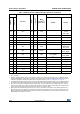
Table 8. General operating conditions
Symbol Parameter Conditions Min Max Unit
f
HCLK
Internal AHB clock frequency 0 48
MHzf
PCLK1
Internal APB1 clock frequency 0 24
f
PCLK2
Internal APB2 clock frequency 0 48
V
DD
Standard operating voltage 2 3.6 V
V
DDA
(1)
1. When the ADC is used, refer to Table 47: ADC characteristics.
Analog operating voltage
(ADC not used)
Must be the same potential
as V
DD
(2)
2. It is recommended to power V
DD
and V
DDA
from the same source. A maximum difference of 300 mV
between V
DD
and V
DDA
can be tolerated during power-up and operation.
23.6
V
Analog operating voltage
(ADC used)
2.4 3.6
V
IN
I/O input voltage
Standard IO –0.3
V
DD
+
0.3
FTIO
(3)
3. To sustain a voltage higher than V
DD
+0.3 V, the internal pull-up/pull-down resistors must be disabled.
2 V < V
DD
≤ 3.6 V –0.3 5.5
V
DD
= 2 V –0.3 5.2
BOOT0 0 5.5
P
D
Power dissipation at T
A
=
85 °C
(4)
4. If T
A
is lower, higher P
D
values are allowed as long as T
J
does not exceed T
J
max (see Table 6.2: Thermal
characteristics on page 73).
LQFP48 363
mW
LQFP64 444
T
A Ambient temperature
Maximu
m power
dissipati
on
–40 85 °C
Low
power
dissipati
on
(5)
5. In low power dissipation state, T
A
can be extended to this range as long as T
J
does not exceed T
J
max
(see Table 6.2: Thermal characteristics on page 73).
–40 105 °C
T
J Junction temperature range –40 105 °C