STM32F102x8 STM32F102xB Medium-density USB access line, ARM-based 32b MCU with 64/128KB Flash, USB FS, 6 timers, ADC & 8 com. interfaces Datasheet - production data Features • Core: ARM 32-bit Cortex™-M3 CPU – 48 MHz maximum frequency, 1.25 DMIPS/MHz (Dhrystone 2.1) performance at 0 WS memory access – Single-cycle multiplication and hardware division • Memories – 64 or 128 Kbytes of Flash memory – 10 or 16 Kbytes of SRAM • Clock, reset and supply management – 2.0 to 3.
Contents STM32F102x8, STM32F102xB Contents 1 Introduction . . . . . . . . . . . . . . . . . . . . . . . . . . . . . . . . . . . . . . . . . . . . . . . . 7 2 Description . . . . . . . . . . . . . . . . . . . . . . . . . . . . . . . . . . . . . . . . . . . . . . . . . 8 2.1 Device overview . . . . . . . . . . . . . . . . . . . . . . . . . . . . . . . . . . . . . . . . . . . . . 9 2.2 Full compatibility throughout the family . . . . . . . . . . . . . . . . . . . . . . . . . . 12 2.3 Overview . . . .
STM32F102x8, STM32F102xB 6 Contents 5.3.13 I/O port characteristics . . . . . . . . . . . . . . . . . . . . . . . . . . . . . . . . . . . . . . 51 5.3.14 NRST pin characteristics . . . . . . . . . . . . . . . . . . . . . . . . . . . . . . . . . . . . 57 5.3.15 TIM timer characteristics . . . . . . . . . . . . . . . . . . . . . . . . . . . . . . . . . . . . 59 5.3.16 Communications interfaces . . . . . . . . . . . . . . . . . . . . . . . . . . . . . . . . . . 59 5.3.
List of tables STM32F102x8, STM32F102xB List of tables Table 1. Table 2. Table 3. Table 4. Table 5. Table 6. Table 7. Table 8. Table 9. Table 10. Table 11. Table 12. Table 13. Table 14. Table 15. Table 16. Table 17. Table 18. Table 19. Table 20. Table 21. Table 22. Table 23. Table 24. Table 25. Table 26. Table 27. Table 28. Table 29. Table 30. Table 31. Table 32. Table 33. Table 34. Table 35. Table 36. Table 37. Table 38. Table 39. Table 40. Table 41. Table 42. Table 43. Table 44. 4/80 Device summary .
STM32F102x8, STM32F102xB Table 45. Table 46. Table 47. Table 48. Table 49. Table 50. Table 51. Table 52. Table 53. Table 54. List of tables ADC characteristics . . . . . . . . . . . . . . . . . . . . . . . . . . . . . . . . . . . . . . . . . . . . . . . . . . . . . . 66 RAIN max for fADC = 12 MHz . . . . . . . . . . . . . . . . . . . . . . . . . . . . . . . . . . . . . . . . . . . . . . . . 67 ADC accuracy - limited test conditions . . . . . . . . . . . . . . . . . . . . . . . . . . . . . . . . . . . . .
List of figures STM32F102x8, STM32F102xB List of figures Figure 1. Figure 2. Figure 3. Figure 4. Figure 5. Figure 6. Figure 7. Figure 8. Figure 9. Figure 10. Figure 11. Figure 12. Figure 13. Figure 14. Figure 15. Figure 16. Figure 17. Figure 18. Figure 19. Figure 20. Figure 21. Figure 22. Figure 23. Figure 24. Figure 25. Figure 26. Figure 27. Figure 28. Figure 29. Figure 30. Figure 31. Figure 32. Figure 33. Figure 34. Figure 35. Figure 36. Figure 37. Figure 38.
STM32F102x8, STM32F102xB 1 Introduction Introduction This datasheet provides the ordering information and mechanical device characteristics of STM32F102x8 and STM32F102xB medium-density USB access line microcontrollers. For more details on the whole STMicroelectronics STM32F102xx family, please refer to Section 2.2: Full compatibility throughout the family. The medium-density STM32F102xx datasheet should be read in conjunction with the low-, medium- and high-density STM32F10xxx reference manual.
Description 2 STM32F102x8, STM32F102xB Description The STM32F102xx medium-density USB access line incorporates the high-performance ARM Cortex™-M3 32-bit RISC core operating at a 48 MHz frequency, high-speed embedded memories (Flash memory of 64 or 128 Kbytes and SRAM of 10 or 16 Kbytes), and an extensive range of enhanced peripherals and I/Os connected to two APB buses.
STM32F102x8, STM32F102xB 2.1 Description Device overview Table 2.
Description STM32F102x8, STM32F102xB Figure 1.
STM32F102x8, STM32F102xB Description Figure 2. Clock tree To Flash prog. if FLITFCLK 8 MHz HSI RC HSI USB Prescaler /1, 1.5 /2 USBCLK to USB interface 48 MHz HCLK to AHB bus, core, memory and DMA 48 MHz max PLLSRC /8 SW PLLMUL HSI ..., x16 x2, x3, x4 PLL SYSCLK AHB Prescaler 48 MHz /1, 2..
Description 2.2 STM32F102x8, STM32F102xB Full compatibility throughout the family The STM32F102xx is a complete family whose members are fully pin-to-pin, software and feature compatible. In the reference manual, the STM32F102x4 and STM32F102x6 are referred to as low-density devices and the STM32F102x8 and STM32F102xB are referred to as medium-density devices. Low-density devices are an extension of the STM32F102x8/B devices, they are specified in the STM32F102x4/6 datasheet.
STM32F102x8, STM32F102xB Description CRC (cyclic redundancy check) calculation unit The CRC (cyclic redundancy check) calculation unit is used to get a CRC code from a 32-bit data word and a fixed generator polynomial. Among other applications, CRC-based techniques are used to verify data transmission or storage integrity. In the scope of the EN/IEC 60335-1 standard, they offer a means of verifying the Flash memory integrity.
Description STM32F102x8, STM32F102xB Boot modes At startup, boot pins are used to select one of five boot options: • Boot from User Flash • Boot from System Memory • Boot from embedded SRAM The boot loader is located in System Memory. It is used to reprogram the Flash memory by using USART1. For further details please refer to AN2606. Power supply schemes • VDD = 2.0 to 3.6 V: External power supply for I/Os and the internal regulator. Provided externally through VDD pins. • VSSA, VDDA = 2.
STM32F102x8, STM32F102xB Description Low-power modes The STM32F102xx medium-density USB access line supports three low-power modes to achieve the best compromise between low power consumption, short startup time and available wakeup sources: • Sleep mode In Sleep mode, only the CPU is stopped. All peripherals continue to operate and can wake up the CPU when an interrupt/event occurs. • Stop mode The Stop mode achieves the lowest power consumption while retaining the content of SRAM and registers.
Description STM32F102x8, STM32F102xB register to generate an alarm. A 20-bit prescaler is used for the time base clock and is by default configured to generate a time base of 1 second from a clock at 32.768 kHz. Independent watchdog The independent watchdog is based on a 12-bit downcounter and 8-bit prescaler. It is clocked from an independent 40 kHz internal RC and as it operates independently from the main clock, it can operate in Stop and Standby modes.
STM32F102x8, STM32F102xB Description Universal synchronous/asynchronous receiver transmitter (USART) The available USART interfaces communicate at up to 2.25 Mbit/s. They provide hardware management of the CTS and RTS signals, support IrDA SIR ENDEC, are ISO 7816 compliant and have LIN Master/Slave capability. The USART interfaces can be served by the DMA controller.
Description STM32F102x8, STM32F102xB The JTAG TMS and TCK pins are shared respectively with SWDIO and SWCLK and a specific sequence on the TMS pin is used to switch between JTAG-DP and SW-DP.
STM32F102x8, STM32F102xB Pinout and pin description VDD_3 VSS_3 PB9 PB8 BOOT0 PB7 PB6 PB5 PB4 PB3 PA15 PA14 Figure 3.
Pinout and pin description STM32F102x8, STM32F102xB Table 4.
STM32F102x8, STM32F102xB Pinout and pin description Table 4.
Pinout and pin description STM32F102x8, STM32F102xB Table 4.
STM32F102x8, STM32F102xB Pinout and pin description 7. The pins number 5 and 6 in the LQFP48 package are configured as OSC_IN/OSC_OUT after reset, however the functionality of PD0 and PD1 can be remapped by software on these pins. For more details, refer to the Alternate function I/O and debug configuration section in the STM32F10xxx reference manual. The use of PD0 and PD1 in output mode is limited as they can only be used at 50 MHz in output mode. 8.
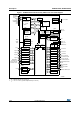
Memory mapping 4 STM32F102x8, STM32F102xB Memory mapping The memory map is shown in Figure 5.
STM32F102x8, STM32F102xB Memory mapping Figure 5.
Electrical characteristics STM32F102x8, STM32F102xB 5 Electrical characteristics 5.1 Parameter conditions Unless otherwise specified, all voltages are referred to VSS. 5.1.1 Minimum and maximum values Unless otherwise specified the minimum and maximum values are guaranteed in the worst conditions of ambient temperature, supply voltage and frequencies by tests in production on 100% of the devices with an ambient temperature at TA = 25 °C and TA = TAmax (given by the selected temperature range).
STM32F102x8, STM32F102xB Electrical characteristics Figure 6. Pin loading conditions Figure 7. Pin input voltage STM32F102 pin STM32F102 pin C = 50 pF VIN ai14973 ai14972 5.1.6 Power supply scheme Figure 8. Power supply scheme VBAT GP I/Os IN VDD VDD VDD 1/2/3/4 Level shifter OUT 3 × 100 nF + 1 × 4.7 µF Backup circuitry (OSC32K,RTC, Wake-up logic Backup registers) Po wer swi tch 1.8-3.
Electrical characteristics 5.1.7 STM32F102x8, STM32F102xB Current consumption measurement Figure 9. Current consumption measurement scheme IDD_VBAT VBAT IDD VDD VDDA ai14126 5.2 Absolute maximum ratings Stresses above the absolute maximum ratings listed in Table 5: Voltage characteristics, Table 6: Current characteristics, and Table 7: Thermal characteristics may cause permanent damage to the device.
STM32F102x8, STM32F102xB Electrical characteristics Table 6. Current characteristics Symbol IVDD IVSS IIO IINJ(PIN) (2) ΣIINJ(PIN) Ratings Max.
Electrical characteristics STM32F102x8, STM32F102xB 5.3 Operating conditions 5.3.1 General operating conditions Table 8. General operating conditions Symbol Parameter fHCLK Min Max Internal AHB clock frequency 0 48 fPCLK1 Internal APB1 clock frequency 0 24 fPCLK2 Internal APB2 clock frequency 0 48 VDD Standard operating voltage 2 3.6 2 3.6 2.4 3.6 –0.3 VDD+ 0.3 2 V < VDD ≤ 3.6 V –0.3 5.5 VDD = 2 V –0.3 5.2 0 5.
STM32F102x8, STM32F102xB 5.3.2 Electrical characteristics Operating conditions at power-up / power-down Subject to general operating conditions for TA. Table 9.
Electrical characteristics 5.3.3 STM32F102x8, STM32F102xB Embedded reset and power control block characteristics The parameters given in Table 11 are derived from tests performed under ambient temperature and VDD supply voltage conditions summarized in Table 8. . Table 10. Embedded reset and power control block characteristics Symbol VPVD VPVDhyst(2) Parameter Conditions Programmable voltage detector level selection Min Typ Max Unit PLS[2:0]=000 (rising edge) 2.1 2.18 2.
STM32F102x8, STM32F102xB Electrical characteristics Table 11. Embedded internal reference voltage Symbol VREFINT Parameter Internal reference voltage TS_vrefint(1) ADC sampling time when reading the internal reference voltage VRERINT(2) Internal reference voltage spread over the temperature range TCoeff(2) Conditions Min Typ –40 °C < TA < +85 °C 1.16 1.20 1.24 V 5.1 17.1(2) µs 10 mV 100 ppm/ °C VDD = 3 V ±10 mV Temperature coefficient Max Unit 1.
Electrical characteristics STM32F102x8, STM32F102xB Table 12. Maximum current consumption in Run mode, code with data processing running from Flash Max(1) Symbol Parameter Conditions External clock (2), all peripherals enabled IDD Supply current in Run mode External clock (2), all peripherals Disabled fHCLK Unit TA = 85 °C 48 MHz 36.1 36 MHz 28.6 24 MHz 19.9 16 MHz 14.7 8 MHz 8.6 48 MHz 24.4 36 MHz 19.8 24 MHz 13.9 16 MHz 10.7 8 MHz 6.8 mA 1.
STM32F102x8, STM32F102xB Electrical characteristics Figure 10. Typical current consumption in Run mode versus temperature (at 3.6 V) code with data processing running from RAM, peripherals enabled 30 Consumption (mA) 25 20 48 MHz 36 MHz 15 16 MHz 8 MHz 10 5 0 -40 0 25 70 85 Temperature (°C) Figure 11. Typical current consumption in Run mode versus temperature (at 3.
Electrical characteristics STM32F102x8, STM32F102xB Table 14. Maximum current consumption in Sleep mode, code running from Flash or RAM Max(1) Symbol Parameter Conditions External clock(2) all peripherals enabled Supply current in Sleep mode IDD External clock(2), all peripherals disabled fHCLK Unit TA = 85 °C 48 MHz 20 36 MHz 15.5 24 MHz 11.5 16 MHz 8.5 8 MHz 5.5 48 MHz 6 36 MHz 5 24 MHz 4.5 16 MHz 4 8 MHz 3 mA 1.
STM32F102x8, STM32F102xB Electrical characteristics 2. To have the Standby consumption with RTC ON, add IDD_VBAT (Low-speed oscillator and RTC ON) to IDD Standby (when VDD is present the Backup Domain is powered by VDD supply). 3. Based on characterization, not tested in production. Figure 12. Typical current consumption on VBAT with RTC on versus temperature at different VBAT values Consumption ( µA ) 2.5 2 2V 1.5 2.4 V 1 3V 0.5 3.
Electrical characteristics STM32F102x8, STM32F102xB Figure 14. Typical current consumption in Stop mode with regulator in Low-power mode versus temperature at VDD = 3.3 V and 3.6 V 140 Consumption (µA) 120 100 80 3.3 V 3.6 V 60 40 20 0 -40 0 25 70 85 Temperature (°C) Figure 15. Typical current consumption in Standby mode versus temperature at VDD = 3.3 V and 3.6 V Standby mode 3 Consumption (µA) 2.5 2 3.3 V 1.5 3.6 V 1 0.
STM32F102x8, STM32F102xB Electrical characteristics Typical current consumption The MCU is placed under the following conditions: • All I/O pins are in input mode with a static value at VDD or VSS (no load) • All peripherals are disabled except if it is explicitly mentioned • The Flash access time is adjusted to fHCLK frequency (0 wait state from 0 to 24 MHz, 1 wait state from 24 to 48 MHz) • Prefetch is on (reminder: this bit must be set before clock setting and bus prescaling) • When the periph
Electrical characteristics STM32F102x8, STM32F102xB 3. External clock is 8 MHz and PLL is on when fHCLK > 8 MHz. Table 17. Typical current consumption in Sleep mode, code running from Flash or RAM Typ(1) Symbol Parameter Conditions External clock(3) IDD Supply current in Sleep mode Running on High Speed Internal RC (HSI), AHB prescaler used to reduce the frequency fHCLK Typ(1) All peripherals All peripherals enabled(2) disabled 48 MHz 9.9 3.9 36 MHz 7.6 3.1 24 MHz 5.3 2.3 16 MHz 3.
STM32F102x8, STM32F102xB Electrical characteristics On-chip peripheral current consumption The current consumption of the on-chip peripherals is given in Table 19.
Electrical characteristics 5.3.6 STM32F102x8, STM32F102xB External clock source characteristics High-speed external user clock generated from an external source The characteristics given in Table 20 result from tests performed using an high-speed external clock source, and under ambient temperature and supply voltage conditions summarized in Table 8. Table 19.
STM32F102x8, STM32F102xB Electrical characteristics Figure 16. High-speed external clock source AC timing diagram VHSEH 90% VHSEL 10% tr(HSE) tf(HSE) tW(HSE) tW(HSE) t THSE External clock source fHSE_ext OSC _IN IL STM32F102xx ai14975b Figure 17.
Electrical characteristics STM32F102x8, STM32F102xB High-speed external clock generated from a crystal/ceramic resonator The high-speed external (HSE) clock can be supplied with a 4 to 16 MHz crystal/ceramic resonator oscillator. All the information given in this paragraph are based on characterization results obtained with typical external components specified in Table 22.
STM32F102x8, STM32F102xB Electrical characteristics Figure 18. Typical application with an 8 MHz crystal Resonator with integrated capacitors CL1 fHSE OSC_IN 8 MH z resonator CL2 REXT(1) RF Bias controlled gain STM32F102xx OSC_OU T ai14977b 1. REXT value depends on the crystal characteristics. Low-speed external clock generated from a crystal/ceramic resonator The low-speed external (LSE) clock can be supplied with a 32.768 kHz crystal/ceramic resonator oscillator.
Electrical characteristics STM32F102x8, STM32F102xB Note: For CL1 and CL2 it is recommended to use high-quality ceramic capacitors in the 5 pF to 15 pF range selected to match the requirements of the crystal or resonator. CL1 and CL2, are usually the same size. The crystal manufacturer typically specifies a load capacitance which is the series combination of CL1 and CL2.
STM32F102x8, STM32F102xB Electrical characteristics 2. Refer to application note AN2868 “STM32F10xxx internal RC oscillator (HSI) calibration” available from the ST website www.st.com. 3. Guaranteed by design, not tested in production. 4. Based on characterization, not tested in production. 5. The actual frequency of HSI oscillator may be impacted by a reflow, but does not drift out of the specified range. low-speed internal (LSI) RC oscillator Table 24.
Electrical characteristics STM32F102x8, STM32F102xB Table 26. PLL characteristics Value Symbol Parameter Unit Min(1) Typ Max(1) PLL input clock(2) 1 8.0 25 MHz PLL input clock duty cycle 40 60 % fPLL_OUT PLL multiplier output clock 16 48 MHz tLOCK PLL lock time 200 µs Jitter Cycle-to-cycle jitter 300 ps fPLL_IN 1. Based on characterization, not tested in production. 2.
STM32F102x8, STM32F102xB 5.3.10 Electrical characteristics EMC characteristics Susceptibility tests are performed on a sample basis during device characterization. Functional EMS (Electromagnetic susceptibility) While a simple application is executed on the device (toggling 2 LEDs through I/O ports). the device is stressed by two electromagnetic events until a failure occurs.
Electrical characteristics STM32F102x8, STM32F102xB Electromagnetic Interference (EMI) The electromagnetic field emitted by the device is monitored while a simple application is executed (toggling 2 LEDs through the I/O ports). This emission test is compliant with IEC 61967-2 standard which specifies the test board and the pin loading. Table 30. EMI characteristics Symbol Parameter SEMI 5.3.11 Peak level Conditions VDD = 3.3 V, TA = 25 °C, Monitored frequency band Max vs.
STM32F102x8, STM32F102xB 5.3.12 Electrical characteristics I/O current injection characteristics As a general rule, current injection to the I/O pins, due to external voltage below VSS or above VDD (for standard, 3 V-capable I/O pins) should be avoided during normal product operation. However, in order to give an indication of the robustness of the microcontroller in cases when abnormal injection accidentally happens, susceptibility tests are performed on a sample basis during device characterization.
Electrical characteristics STM32F102x8, STM32F102xB Table 34. I/O static characteristics Symbol Parameter Conditions Standard IO input low level voltage VIL Low level input voltage IO FT(3) input low level voltage All I/Os except BOOT0 Standard IO input high level voltage VIH Vhys Ilkg Min Typ Max - - 0.28*(VDD-2 V)+0.8 V(1) - - 0.32*(VDD-2V)+0.75 V(1) - - 0.35VDD(2) V 0.41*(VDD-2 V)+1.3 V (1) - - IO FT(3) input high level voltage 0.
STM32F102x8, STM32F102xB Electrical characteristics All I/Os are CMOS and TTL compliant (no software configuration required). Their characteristics cover more than the strict CMOS-technology or TTL parameters. The coverage of these requirements is shown in Figure 20 and Figure 21 for standard I/Os, and in Figure 22 and Figure 23 for 5 V tolerant I/Os. Figure 20. Standard I/O input characteristics - CMOS port Area not determined VIH/VIL (V) =0.
Electrical characteristics STM32F102x8, STM32F102xB Figure 22. 5 V tolerant I/O input characteristics - CMOS port Area not determined VIH/VIL (V) =0.65V DD nts V IH quireme dard re OS stan CM Tested ction in produ 1.3 1.295 0.975 1 0.7 0.75 1.55 1.16 -2)+1 V IH=0.42(V DD simulations gn si de on d 1.67 Base -2)+0.75 1 V IL=0.32(V DD ions sign simulat Based on de 1.42 1.07 5V DD ent V IL =0.3 dard requirm CMOS stan oduction Tested in pr 2 2.7 3 3.3 VDD (V) 3.
STM32F102x8, STM32F102xB Electrical characteristics Output voltage levels Unless otherwise specified, the parameters given in Table 37 are derived from tests performed under ambient temperature and VDD supply voltage conditions summarized in Table 8. All I/Os are CMOS and TTL compliant. Table 35.
Electrical characteristics STM32F102x8, STM32F102xB Input/output AC characteristics The definition and values of input/output AC characteristics are given in Figure 24 and Table 38, respectively. Unless otherwise specified, the parameters given in Table 38 are derived from tests performed under ambient temperature and VDD supply voltage conditions summarized in Table 8. Table 36.
STM32F102x8, STM32F102xB Electrical characteristics Figure 24. I/O AC characteristics definition 90% 10% 50% 50% 90% 10% EXTERNAL OUTPUT ON 50pF tr(IO)out tf(IO)out T Maximum frequency is achieved if (tr + tf) ≤ 2/3)T and if the duty cycle is (45-55%) when loaded by 50pF ai14131c 5.3.14 NRST pin characteristics The NRST pin input driver uses CMOS technology. It is connected to a permanent pull-up resistor, RPU (see Table 36).
Electrical characteristics STM32F102x8, STM32F102xB Figure 25. Recommended NRST pin protection VDD External reset circuit(1) NRST(2) RPU Internal Reset Filter 0.1 μF STM32Fxxx ai14132c 1. The reset network protects the device against parasitic resets. 2. The user must ensure that the level on the NRST pin can go below the VIL(NRST) max level specified in Table 39. Otherwise the reset will not be taken into account by the device.
STM32F102x8, STM32F102xB 5.3.15 Electrical characteristics TIM timer characteristics The parameters given in Table 40 are guaranteed by design. Refer to Section 5.3.13: I/O port characteristics for details on the input/output alternate function characteristics (output compare, input capture, external clock, PWM output). Table 38.
Electrical characteristics STM32F102x8, STM32F102xB Table 39. I2C characteristics Standard mode I2C(1) Fast mode I2C(1)(2) Symbol Parameter Unit Min Max Min tw(SCLL) SCL clock low time 4.7 1.3 tw(SCLH) SCL clock high time 4.0 0.6 tsu(SDA) SDA setup time 250 Max µs 100 (3) 0 900(3) 20+0.1Cb 300 th(SDA) SDA data hold time tr(SDA) tr(SCL) SDA and SCL rise time 1000 tf(SDA) tf(SCL) SDA and SCL fall time 300 th(STA) Start condition hold time 4.0 0.
STM32F102x8, STM32F102xB Electrical characteristics Figure 26. I2C bus AC waveforms and measurement circuit(1) VDD_I2C VDD_I2C Rp Rp STM32F10x Rs SDA I²C bus Rs SCL Start repeated Start Start tsu(STA) SDA tf(SDA) tr(SDA) th(STA) tsu(SDA) tw(SCLL) th(SDA) tsu(STO:STA) Stop SCL tw(SCLH) tr(SCL) tf(SCL) tsu(STO) ai14133e 1. Measurement points are done at CMOS levels: 0.3VDD and 0.7VDD. Table 40. SCL frequency (fPCLK1= 36 MHz, VDD_I2C = 3.3 V)(1)(2) fSCL I2C_CCR value (kHz) RP = 4.
Electrical characteristics STM32F102x8, STM32F102xB SPI interface characteristics Unless otherwise specified, the parameters given in Table 43 are derived from tests performed under ambient temperature, fPCLKx frequency and VDD supply voltage conditions summarized in Table 8. Refer to Section 5.3.13: I/O port characteristics for more details on the input/output alternate function characteristics (NSS, SCK, MOSI, MISO). Table 41.
STM32F102x8, STM32F102xB Electrical characteristics Figure 27. SPI timing diagram - slave mode and CPHA=0 NSS input tc(SCK) th(NSS) SCK Input tSU(NSS) CPHA= 0 CPOL=0 tw(SCKH) tw(SCKL) CPHA= 0 CPOL=1 tv(SO) ta(SO) MISO OUT P UT tr(SCK) tf(SCK) th(SO) MS B O UT BI T6 OUT tdis(SO) LSB OUT tsu(SI) MOSI I NPUT M SB IN LSB IN B I T1 IN th(SI) ai14134c Figure 28.
Electrical characteristics STM32F102x8, STM32F102xB Figure 29. SPI timing diagram - master mode(1) High NSS input SCK Output CPHA= 0 CPOL=0 SCK Output tc(SCK) CPHA=1 CPOL=0 CPHA= 0 CPOL=1 CPHA=1 CPOL=1 tsu(MI) MISO INP UT tw(SCKH) tw(SCKL) tr(SCK) tf(SCK) MS BIN BI T6 IN LSB IN th(MI) MOSI OUTUT B I T1 OUT M SB OUT tv(MO) LSB OUT th(MO) ai14136V2 1. Measurement points are done at CMOS levels: 0.3VDD and 0.7VDD. USB characteristics The USB interface is USB-IF certified (Full Speed).
STM32F102x8, STM32F102xB Electrical characteristics Table 43. USB DC electrical characteristics Symbol Parameter VDD Input levels VDI (4) VCM(4) Min.(1) Conditions USB operating voltage(2) 3.0(3) Differential input sensitivity VOL VOH V V 0.2 Includes VDI range 0.8 2.5 1.3 2.0 Differential common mode range RL of 1.5 kΩ to 3.6 V(5) Static output level low RL of 15 kΩ to Static output level high 3.6 I(USB_DP, USB_DM) VSE(4) Single ended receiver threshold Output levels Max.
Electrical characteristics STM32F102x8, STM32F102xB Table 45. ADC characteristics Symbol Parameter Conditions Min Typ Max Unit VDDA Power supply 2.4 3.6 V fADC ADC clock frequency 0.6 12 MHz fS(1) Sampling rate 0.05 0.
STM32F102x8, STM32F102xB Electrical characteristics Table 46. RAIN max for fADC = 12 MHz(1) Ts (cycles) tS (µs) RAIN max (kΩ) 1.5 0.13 0.4 7.5 0.63 5.9 13.5 1.13 11.4 28.5 2.38 25.2 41.5 3.46 37.2 55.5 4.63 50 71.5 5.96 NA 239.5 19.96 NA 1. Data guaranteed by design, not tested in production. Table 47.
Electrical characteristics STM32F102x8, STM32F102xB Figure 31. ADC accuracy characteristics [1LSBIDEAL = VDDA 4096 EG (1) Example of an actual transfer curve (2) The ideal transfer curve (3) End point correlation line 4095 4094 4093 (2) ET 7 (1) 6 5 4 ET=Total u nadjusted er ror: maximum deviation between the actual and the ideal transfer curves. EO=Offset e rror: deviation between the first actual transition and the first ideal one.
STM32F102x8, STM32F102xB Electrical characteristics General PCB design guidelines Power supply decoupling should be performed as shown in Figure 33. The 10 nF capacitors should be ceramic (good quality). They should be placed as close as possible to the chip. Figure 33. Power supply and reference decoupling STM32F102xx VDDA 1 µF // 10 nF VSSA ai14980b 5.3.18 Temperature sensor characteristics Table 49.
Package characteristics STM32F102x8, STM32F102xB 6 Package characteristics 6.1 Package mechanical data In order to meet environmental requirements, ST offers these devices in different grades of ECOPACK® packages, depending on their level of environmental compliance. ECOPACK® specifications, grade definitions and product status are available at: www.st.com. ECOPACK® is an ST trademark. Figure 34. LQFP64 – 10 x 10 mm, 48-pin low-profile quad flat package outline A2 c A1 A SEATING PLANE C 0.
STM32F102x8, STM32F102xB Package characteristics Table 50. LQFP64 – 10 x 10 mm, 64-pin low-profile quad flat package mechanical data inches(1) millimeters Symbol Min Typ Max A Min Typ 1.600 A1 0.050 A2 1.350 b 0.170 c 0.090 D 11.800 D1 9.800 Max 0.0630 0.150 0.0020 1.400 1.450 0.0531 0.0551 0.0571 0.220 0.270 0.0067 0.0087 0.0106 0.200 0.0035 12.000 12.200 0.4646 0.4724 0.4803 10.000 10.200 0.3858 0.3937 0.4016 D3 0.0059 0.0079 7.50 0.2953 E 11.800 12.
Package characteristics STM32F102x8, STM32F102xB Figure 36. LQFP48 – 7 x 7 mm, 48-pin low-profile quad flat package outline c A1 A A2 SEATING PLANE C 0.25 mm GAUGE PLANE ccc C K A1 D L D1 L1 D3 36 25 37 24 48 PIN 1 IDENTIFICATION E 13 1 12 e 1. Drawing is not to scale. 2. Dimensions are in millimeters.
STM32F102x8, STM32F102xB Package characteristics Table 51. LQFP48 – 7 x 7 mm, 48-pin low-profile quad flat package mechanical data inches(1) millimeters Symbol Min Typ Max A Min Typ 1.600 A1 0.050 A2 1.350 b 0.170 c 0.090 D 8.800 D1 6.800 D3 Max 0.0630 0.150 0.0020 0.0059 1.400 1.450 0.0531 0.0551 0.0571 0.220 0.270 0.0067 0.0087 0.0106 0.200 0.0035 9.000 9.200 0.3465 0.3543 0.3622 7.000 7.200 0.2677 0.2756 0.2835 0.0079 5.500 0.2165 E 8.800 9.000 9.
Package characteristics 6.2 STM32F102x8, STM32F102xB Thermal characteristics The maximum chip junction temperature (TJmax) must never exceed the values given in Table 8: General operating conditions on page 30.
STM32F102x8, STM32F102xB Evaluating the maximum junction temperature for an application When ordering the microcontroller, the temperature range is specified in the ordering information scheme shown in Table 55: Ordering information scheme. Each temperature range suffix corresponds to a specific guaranteed ambient temperature at maximum dissipation and, to a specific maximum junction temperature. Here, only temperature range 6 is available (–40 to 85 °C).
Ordering information scheme 7 STM32F102x8, STM32F102xB Ordering information scheme Table 53. Ordering information scheme Example: STM32 F 102 C 8 Device family STM32 = ARM-based 32-bit microcontroller Product type F = general-purpose Device subfamily 102 = USB access line, USB 2.0 full-speed interface Pin count C = 48 pins R = 64 pins Flash memory size 8 = 64 Kbytes of Flash memory B = 128 Kbytes of Flash memory Package T = LQFP Temperature range 6 = Industrial temperature range, –40 to 85 °C.
STM32F102x8, STM32F102xB 8 Revision history Revision history Table 54. Document revision history Date Revision 23-Sep-2008 1 Initial release. 2 I/O information clarified on page 1. Figure 1: STM32F102T8 mediumdensity USB access line block diagram and Figure 5: Memory map modified. In Table 4: Medium-density STM32F102xx pin definitions: PB4, PB13, PB14, PB15, PB3/TRACESWO moved from Default column to Remap column. PD value added for LQFP64 package in Table 8: General operating conditions.
Revision history STM32F102x8, STM32F102xB Table 54. Document revision history (continued) Date 27-Sep-2012 78/80 Revision Changes 4 Figure 2: Clock tree: added FLITFCLK and Note 3., and modified Note 1.. Updated Note 2. in Table 41: I2C characteristics. Updated Figure 25: Recommended NRST pin protection. Changed tw(SCKH) to tw(SCLH), tw(SCKL) to tw(SCLL), tr(SCK) to tr(SCL), tf(SCK) to tf(SCL), and tsu(STA:STO) to tw(STO:STA) in Figure 26: I2C bus AC waveforms and measurement circuit(1).
STM32F102x8, STM32F102xB Revision history Table 54. Document revision history (continued) Date 02-Aug-2013 Revision Changes 5 Removed sentence in “Unless otherwise specified the parameters ...” in I2C interface characteristics section. Added VIN in Table 8: General operating conditions Added note 5.
STM32F102x8, STM32F102xB Please Read Carefully: Information in this document is provided solely in connection with ST products. STMicroelectronics NV and its subsidiaries (“ST”) reserve the right to make changes, corrections, modifications or improvements, to this document, and the products and services described herein at any time, without notice. All ST products are sold pursuant to ST’s terms and conditions of sale.