
Datasheet


STM32F101xF, STM32F101xG Electrical characteristics
Doc ID 17143 Rev 2 97/108
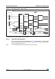
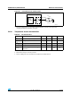
Figure 52. Power supply and reference decoupling (V
REF+
connected to V
DDA
)
1. V
REF+
and V
REF-
inputs are available only on 100-pin packages.
5.3.19 DAC electrical specifications
V
REF+
/V
DDA
STM32F10xxx
1 µF // 10 nF
V
REF–
/V
SSA
ai14381b
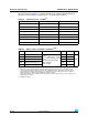
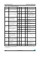
Table 59. DAC characteristics
Symbol Parameter Min Typ Max
(1)
Unit Comments
V
DDA
Analog supply voltage 2.4 3.6 V
V
REF+
Reference supply voltage 2.4 3.6 V
V
REF+
must always be below
V
DDA
V
SSA
Ground 0 0 V
R
LOAD
(2)
Resistive load with buffer ON 5 k
R
O
(2)
Impedance output with buffer
OFF
15 k
When the buffer is OFF, the
minimum resistive load
between DAC_OUT and V
SS
to
have a 1% accuracy is 1.5 M
C
LOAD
(2)
Capacitive load 50 pF
Maximum capacitive load at
DAC_OUT pin (when the buffer
is ON).
DAC_OUT
min
(2)
Lower DAC_OUT voltage with
buffer ON
0.2 V
It gives the maximum output
excursion of the DAC.
It corresponds to 12-bit input
code (0x0E0) to (0xF1C) at
V
REF+
= 3.6 V and (0x155) and
(0xEAB) at V
REF+
= 2.4 V.
DAC_OUT
max
(2)
Higher DAC_OUT voltage with
buffer ON
V
DDA
– 0.2 V
DAC_OUT
min
(2)
Lower DAC_OUT voltage with
buffer OFF
0.5 mV
It gives the maximum output
excursion of the DAC.
DAC_OUT
max
(2)
Higher DAC_OUT voltage with
buffer OFF
V
REF+
– 1LSB V