
Datasheet


STM32F101xF, STM32F101xG Electrical characteristics
Doc ID 17143 Rev 2 95/108
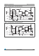
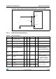
Figure 49. ADC accuracy characteristics
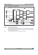
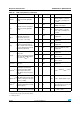
Table 58. ADC accuracy
(1)
(2)(3)
1. ADC DC accuracy values are measured after internal calibration.
2. Better performance could be achieved in restricted V
DD
, frequency, V
REF
and temperature ranges.
3. ADC accuracy vs. negative injection current: Injecting negative current on any of the standard (non-robust)
analog input pins should be avoided as this significantly reduces the accuracy of the conversion being
performed on another analog input. It is recommended to add a Schottky diode (pin to ground) to standard
analog pins which may potentially inject negative current.
Any positive injection current within the limits specified for I
INJ(PIN)
and I
INJ(PIN)
in Section 5.3.14 does not
affect the ADC accuracy.
Symbol Parameter Test conditions Typ Max
(4)
4. Preliminary values.
Unit
ET Total unadjusted error
f
PCLK2
= 28 MHz,
f
ADC
= 14 MHz, R
AIN
< 10 k,
V
DDA
= 2.4 V to 3.6 V
Measurements made after
ADC calibration
±2 ±5
LSB
EO Offset error ±1.5 ±2.5
EG Gain error ±1.5 ±3
ED Differential linearity error ±1 ±2
EL Integral linearity error ±1.5 ±3
E
O
E
G
1LSB
IDEAL
(1) Example of an actual transfer curve
(2) The ideal transfer curve
(3) End point correlation line
E
T
=Total Unadjusted Error: maximum deviation
between the actual and the ideal transfer curves.
E
O
=Offset Error: deviation between the first actual
transition and the first ideal one.
E
G
=Gain Error: deviation between the last ideal
transition and the last actual one.
E
D
=Differential Linearity Error: maximum deviation
between actual steps and the ideal one.
E
L
=Integral Linearity Error: maximum deviation
between any actual transition and the end point
correlation line.
4095
4094
4093
5
4
3
2
1
0
7
6
1234567
4093 4094 4095 4096
(1)
(2)
E
T
E
D
E
L
(3)
V
DDA
V
SSA
ai14395b
V
REF+
4096
(or depending on package)]
V
DDA
4096
[1LSB
IDEAL
=