
Datasheet


Electrical characteristics STM32F101xF, STM32F101xG
56/108 Doc ID 17143 Rev 2
5.3.8 PLL characteristics
The parameters given in Ta ble 2 8 are derived from tests performed under ambient
temperature and V
DD
supply voltage conditions summarized in Table 10 .
5.3.9 Memory characteristics
Flash memory
The characteristics are given at T
A
= –40 to 85 °C unless otherwise specified.
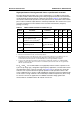
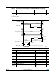
Table 28. PLL characteristics
Symbol Parameter
Value
Unit
Min
(1)
Typ Max
(1)
1. Based on characterization, not tested in production.
f
PLL_IN
PLL input clock
(2)
2. Take care of using the appropriate multiplier factors so as to have PLL input clock values compatible with
the range defined by f
PLL_OUT
.
18.025MHz
PLL input clock duty cycle 40 60 %
f
PLL_OUT
PLL multiplier output clock 16 36 MHz
t
LOCK
PLL lock time 200 µs
Jitter Cycle-to-cycle jitter 300 ps
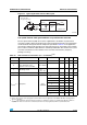
Table 29. Flash memory characteristics
Symbol Parameter Conditions Min Typ Max
(1)
1. Guaranteed by design, not tested in production.
Unit
t
prog
16-bit programming time T
A
–40 to +85 °C 40 52.5 70 µs
t
ERASE
Page (2 KB) erase time T
A
–40 to +85 °C 20 40 ms
t
ME
Mass erase time T
A
–40 to +85 °C 20 40 ms
I
DD
Supply current
Read mode
f
HCLK
= 36 MHz with 1
wait state, V
DD
= 3.3 V
28 mA
Write mode
f
HCLK
= 36 MHz, V
DD
=
3.3 V
7mA
Erase mode
f
HCLK
= 36 MHz, V
DD
=
3.3 V
5mA
Power-down mode / Halt,
V
DD
= 3.0 to 3.6 V
50 µA
V
prog
Programming voltage 2 3.6 V