
Datasheet


STM32F101xF, STM32F101xG Electrical characteristics
Doc ID 17143 Rev 2 37/108
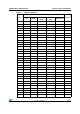
Table 8. Current characteristics
Symbol Ratings Max. Unit
I
VDD
Total current into V
DD
/V
DDA
power lines (source)
(1)
1. All main power (V
DD
, V
DDA
) and ground (V
SS
, V
SSA
) pins must always be connected to the external power
supply, in the permitted range.
150
mA
I
VSS
Total current out of V
SS
ground lines (sink)
(1)
150
I
IO
Output current sunk by any I/O and control pin 25
Output current source by any I/Os and control pin 25
I
INJ(PIN)
(2)
2. Negative injection disturbs the analog performance of the device. See note in Section 5.3.18: 12-bit ADC
characteristics.
Injected current on five volt tolerant pins
(3)
3. Positive injection is not possible on these I/Os. V
IN
maximum must always be respected. I
INJ(PIN)
must
never be exceeded. A negative injection is induced by V
IN
<V
SS
.
-5/+0
Injected current on any other pin
(4)
4. I
INJ(PIN)
must never be exceeded. This is implicitly insured if V
IN
maximum is respected. If V
IN
maximum
cannot be respected, the injection current must be limited externally to the I
INJ(PIN)
value. A positive
injection is induced by V
IN
>V
DD
while a negative injection is induced by V
IN
<V
SS
.
± 5
I
INJ(PIN)
Total injected current (sum of all I/O and control pins)
(5)
5. When several inputs are submitted to a current injection, the maximum I
INJ(PIN)
is the absolute sum of the
positive and negative injected currents (instantaneous values). These results are based on
characterization with I
INJ(PIN)
maximum current injection on four I/O port pins of the device.
± 25
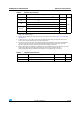
Table 9. Thermal characteristics
Symbol Ratings Value Unit
T
STG
Storage temperature range –65 to +150 °C
T
J
Maximum junction temperature 150 °C