
Datasheet


Electrical characteristics STM32F101xF, STM32F101xG
36/108 Doc ID 17143 Rev 2
5.1.7 Current consumption measurement
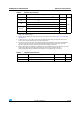
Figure 10. Current consumption measurement scheme
5.2 Absolute maximum ratings
Stresses above the absolute maximum ratings listed in Table 7: Voltage characteristics,
Table 8: Current characteristics, and Table 9: Thermal characteristics may cause permanent
damage to the device. These are stress ratings only and functional operation of the device
at these conditions is not implied. Exposure to maximum rating conditions for extended
periods may affect device reliability.
ai14126
V
BAT
V
DD
V
DDA
I
DD
_V
BAT
I
DD
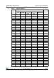
Table 7. Voltage characteristics
Symbol Ratings Min Max Unit
V
DD
V
SS
External main supply voltage (including
V
DDA
and V
DD
)
(1)
1. All main power (V
DD
, V
DDA
) and ground (V
SS
, V
SSA
) pins must always be connected to the external power
supply, in the permitted range.
–0.3 4.0
V
V
IN
Input voltage on five volt tolerant pin
(2)
2. Positive injection is not possible on these I/Os. V
IN
maximum must always be respected. I
INJ(PIN)
must
never be exceeded. A negative injection is induced by V
IN
<V
SS
.
V
SS
0.3 V
DD
+4 V
Input voltage on any other pin
(3)
3. I
INJ(PIN)
must never be exceeded. This is implicitly insured if V
IN
maximum is respected. If V
IN
maximum
cannot be respected, the injection current must be limited externally to the I
INJ(PIN)
value. A positive
injection is induced by V
IN
>V
DD
while a negative injection is induced by V
IN
<V
SS
V
SS
0.3 4.0
|V
DDx
| Variations between different V
DD
power pins 50
mV
|V
SSX
V
SS
|
Variations between all the different ground
pins
50
V
ESD(HBM)
Electrostatic discharge voltage (human body
model)
see Section 5.3.12: Absolute
maximum ratings (electrical
sensitivity)