
Datasheet


Pinouts and pin descriptions STM32F101xF, STM32F101xG
30/108 Doc ID 17143 Rev 2
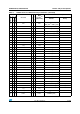
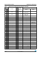
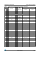
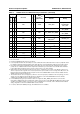
133 55 89
PB3 I/O FT JTDO SPI3_SCK
TIM2_CH2 /
PB3
TRACESWO
SPI1_SCK
134 56 90
PB4 I/O FT NJTRST SPI3_MISO
PB4 /
TIM3_CH1
SPI1_MISO
135 57 91 PB5 I/O PB5 I2C1_SMBA/ SPI3_MOSI
TIM3_CH2 /
SPI1_MOSI
136 58 92 PB6 I/O FT PB6 I2C1_SCL / TIM4_CH1
(7)
USART1_TX
137 59 93 PB7 I/O FT PB7
I2C1_SDA / FSMC_NADV /
TIM4_CH2
(7)
USART1_RX
138 60 94 BOOT0 I BOOT0
139 61 95 PB8 I/O FT PB8 TIM4_CH3
(7)
I2C1_SCL
140 62 96 PB9 I/O FT PB9 TIM4_CH4
(7)
I2C1_SDA
141 - 97 PE0 I/O FT PE0 TIM4_ETR
(7)
/ FSMC_NBL0
142 - 98 PE1 I/O FT PE1 FSMC_NBL1
143 63 99 V
SS_3
SV
SS_3
144 64 100 V
DD_3
SV
DD_3
1. I = input, O = output, S = supply.
2. FT = 5 V tolerant.
3. Function availability depends on the chosen device.
4. If several peripherals share the same I/O pin, to avoid conflict between these alternate functions only one peripheral should
be enabled at a time through the peripheral clock enable bit (in the corresponding RCC peripheral clock enable register).
5. PC13, PC14 and PC15 are supplied through the power switch. Since the switch only sinks a limited amount of current
(3 mA), the use of GPIOs PC13 to PC15 in output mode is limited: the speed should not exceed 2 MHz with a maximum
load of 30 pF and these IOs must not be used as a current source (e.g. to drive an LED).
6. Main function after the first backup domain power-up. Later on, it depends on the contents of the Backup registers even
after reset (because these registers are not reset by the main reset). For details on how to manage these IOs, refer to the
Battery backup domain and BKP register description sections in the STM32F10xxx reference manual, available from the
STMicroelectronics website: www.st.com.
7. This alternate function can be remapped by software to some other port pins (if available on the used package). For more
details, refer to the Alternate function I/O and debug configuration section in the STM32F10xxx reference manual,
available from the STMicroelectronics website: www.st.com.
8. For the LQFP64 package, the pins number 5 and 6 are configured as OSC_IN/OSC_OUT after reset, however the
functionality of PD0 and PD1 can be remapped by software on these pins. For the LQFP100 and LQFP144 packages, PD0
and PD1 are available by default, so there is no need for remapping. For more details, refer to Alternate function I/O and
debug configuration section in the STM32F10xxx reference manual
9. For devices delivered in LQFP64 packages, the FSMC function is not available.
Table 5. STM32F101xF and STM32F101xG pin definitions (continued)
Pins
Pin name
Type
(1)
I / O level
(2)
Main
function
(3)
(after reset)
Alternate functions
(4)
LQFP144
LQFP64
LQFP100
Default Remap