
Datasheet


DocID13586 Rev 16 85/90
STM32F101x8, STM32F101xB Revision history
89
22-Nov-2007 4
Document status promoted from preliminary data to datasheet. Small text
changes.
STM32F101CB part number corrected in Table 1: Device summary.
Number of communication peripherals corrected for STM32F101Tx in
Table 2: Device features and peripheral counts (STM32F101xx medium-
density access line) and Number of GPIOs corrected for LQFP package.
Power supply schemes on page 16 modified.
Main function and default alternate function modified for PC14 and PC15
in Table 4: Medium-density STM32F101xx pin definitions, Note 6 added,
Remap column added.
Figure 11: Power supply scheme modified. V
DD
V
SS
ratings modified
and Note 1 modified in Table 5: Voltage characteristics. Note 1 modified in
Table 6: Current characteristics.
Note 2 added in Table 10: Embedded reset and power control block
characteristics.
48 and 72 MHz frequencies removed from Table 12, Tab le 13 and
Table 14. MCU ‘s operating conditions modified in Typical current
consumption on page 42.
I
DD_VBAT
typical value at 2.4 V modified and I
DD_VBAT
maximum value
added in Table 15: Typical and maximum current consumptions in Stop
and Standby modes. Note added in Table 16 on page 42 and Table 17 on
page 43. Table 18: Peripheral current consumption modified.
Figure 17: Typical current consumption in Stop mode with regulator in
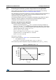
Low-power mode versus temperature at VDD = 3.3 V and 3.6 V added.
Note removed below Figure 30: SPI timing diagram - slave mode and
CPHA = 0. Note added below Figure 31: SPI timing diagram - slave mode
and CPHA = 1(1).
Figure 34: Typical connection diagram using the ADC modified.
t
SU(HSE)
and t
SU(LSE)
conditions modified in Table 21 and Table 22,
respectively. Maximum values removed from Table 25: Low-power mode
wakeup timings. t
RET
conditions modified in Table 28: Flash memory
endurance and data retention. Conditions modified in Table 29: EMS
characteristics.
Impedance size specified in A.4: Voltage glitch on ADC input 0 on
page 71. Small text changes in Table 35: Output voltage characteristics.
Section 5.3.11: Absolute maximum ratings (electrical sensitivity) updated.
Details on unused pins removed from General input/output characteristics
on page 55.
Table 41: SPI characteristics updated. Notes added and I
lkg
removed in
Table 42: ADC characteristics. Note added in Table 43 and Tab le 46.
Note 3 and Note 2 added below Table 44: ADC accuracy - limited test
conditions. Avg_Slope and V
25
modified in Table 46: TS characteristics.
JA
value for VFQFPN36 package added in Table 52: Package thermal
characteristicsI2C interface characteristics on page 62 modified.
Order codes replaced by Section 7: Ordering information scheme.
Table 54. Document revision history (continued)
Date Revision Changes