
Datasheet


Electrical characteristics STM32F101x8, STM32F101xB
36/90 DocID13586 Rev 16
5.3.4 Embedded reference voltage
The parameters given in Table 11 are derived from tests performed under the ambient
temperature and V
DD
supply voltage conditions summarized in Table 8.
5.3.5 Supply current characteristics
The current consumption is a function of several parameters and factors such as the
operating voltage, ambient temperature, I/O pin loading, device software configuration,
operating frequencies, I/O pin switching rate, program location in memory and executed
binary code.
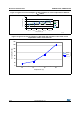
The current consumption is measured as described in Figure 12: Current consumption
measurement scheme.
All Run-mode current consumption measurements given in this section are performed with a
reduced code that gives a consumption equivalent to Dhrystone 2.1 code.
Maximum current consumption
The MCU is placed under the following conditions:
All I/O pins are in input mode with a static value at V
DD
or V
SS
(no load)
All peripherals are disabled except if it is explicitly mentioned
The Flash access time is adjusted to f
HCLK
frequency (0 wait state from 0 to 24 MHz, 1
wait state from 24 to 36 MHz)
Prefetch in on (reminder: this bit must be set before clock setting and bus prescaling)
When the peripherals are enabled f
PCLK1
= f
HCLK/2
, f
PCLK2
= f
HCLK
The parameters given in Table 12 are derived from tests performed under the ambient
temperature and V
DD
supply voltage conditions summarized in Table 8.
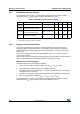
Table 11. Embedded internal reference voltage
Symbol Parameter Conditions Min Typ Max Unit
V
REFINT
Internal reference voltage –40 °C < T
A
< +85 °C 1.16 1.20 1.24 V
T
S_vrefint
(1)
1. Shortest sampling time can be determined in the application by multiple iterations.
ADC sampling time when reading
the internal reference voltage
5.1
17.1
(2)
2. Guaranteed by design, not tested in production.
µs
V
RERINT
(2)
Internal reference voltage spread
over the temperature range
V
DD
= 3 V ±10 mV 10 mV
T
Coeff
(2)
Temperature coefficient 100
ppm/
°C