
Datasheet


STM32F101xC, STM32F101xD, STM32F101xE Description
Doc ID 14610 Rev 8 13/112
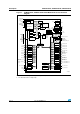
Figure 2. Clock tree
1. When the HSI is used as a PLL clock input, the maximum system clock frequency that can be achieved is
36 MHz.
2. To have an ADC conversion time of 1 µs, APB2 must be at 14 MHz or 28 MHz.
HSE OSC
4-16 MHz
OSC_IN
OSC_OUT
OSC32_IN
OSC32_OUT
LSE OSC
32.768 kHz
HSI RC
8 MHz
LSI RC
40 kHz
to Independent Watchdog (IWDG)
PLL
x2, x3, x4
PLLMUL
HSE = High Speed External clock signal
LSE = Low Speed External clock signal
LSI = Low Speed Internal clock signal
HSI = High Speed Internal clock signal
Legend:
MCO
Clock Output
Main
PLLXTPRE
/2
..., x16
AHB
Prescaler
/1, 2..512
/2
PLLCLK
HSI
HSE
APB1
Prescaler
/1, 2, 4, 8, 16
ADC
Prescaler
/2, 4, 6, 8
ADCCLK
PCLK1
HCLK
PLLCLK
to AHB bus, core,
memory and DMA
to ADC
LSE
LSI
HSI
/128
/2
HSI
HSE
peripherals
to APB1
Peripheral Clock
Enable (18 bits)
Enable (6 bits)
Peripheral Clock
APB2
Prescaler
/1, 2, 4, 8, 16
PCLK2
peripherals to APB2
Peripheral Clock
Enable (11 bits)
36 MHz max
36 MHz
36 MHz max
36 MHz max
to RTC
PLLSRC
SW
MCO
CSS
to Cortex System timer
/8
Clock
Enable (7 bits)
SYSCLK
max
RTCCLK
RTCSEL[1:0]
TIMXCLK
IWDGCLK
SYSCLK
FCLK Cortex
free running clock
TIM2,3,4,5,6,7
to TIM2,3,4,5,6 and 7
to FSMC
FSMCCLK
Peripheral clock
enable
ai15100
If (APB1 prescaler =1) x1
else x2
FLITFCLK
to Flash programming interface