
Datasheet


STM32F101x4, STM32F101x6 Revision history
Doc ID 15058 Rev 5 77/79
8 Revision history
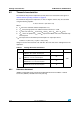
Table 53. Document revision history
Date Revision Changes
23-Sep-2008 1 Initial release.
07-Apr-2009 2
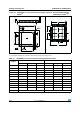
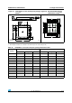
I/O information clarified on page 1. Figure 7: Memory map modified.
In Table 4: Low-density STM32F101xx pin definitions: PB4, PB13, PB14,
PB15, PB3/TRACESWO moved from Default column to Remap column.
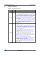
V
REF-
is not available in the offered packages: Figure 1: STM32F101xx
Low-density access line block diagram, Figure 10: Power supply scheme
and Figure 34: Power supply and reference decoupling updated,
Figure 30: Power supply and reference decoupling (V
REF+
not connected
to V
DDA
) removed.
Note modified in Table 12: Maximum current consumption in Run mode,
code with data processing running from Flash and Table 14: Maximum
current consumption in Sleep mode, code running from Flash or RAM.
Figure 15, Figure 16 and Figure 17 show typical curves.
ACC
HSI
max values modified in Table 23: HSI oscillator characteristics.
Small text changes.
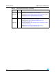
24-Sep-2009 3
Note 5 updated and Note 4 added in Table 4: Low-density
STM32F101xx pin definitions.
V
RERINT
and T
Coeff
added to Table 11: Embedded internal reference
voltage. Typical I
DD_VBAT
value added in Table 15: Typical and maximum
current consumptions in Stop and Standby modes. Figure 14: Typical
current consumption on VBAT with RTC on versus temperature at
different VBAT values added.
f
HSE_ext
min modified in Table 19: High-speed external user clock
characteristics.
C
L1
and C
L2
replaced by C in Table 21: HSE 4-16 MHz oscillator
characteristics and Table 22: LSE oscillator characteristics (fLSE =
32.768 kHz), notes modified and moved below the tables.
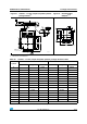
Note 1 modified below Figure 20: Typical application with an 8 MHz
crystal.
Table 23: HSI oscillator characteristics modified. Conditions removed
from Table 25: Low-power mode wakeup timings.
Figure 27: Recommended NRST pin protection modified.
IEC 1000 standard updated to IEC 61000 and SAE J1752/3 updated to
IEC 61967-2 in Section 5.3.10: EMC characteristics on page 48.
Jitter added to Table 26: PLL characteristics.
C
ADC
and R
AIN
parameters modified in Table 42: ADC characteristics.
R
AIN
max values modified in Table 43: RAIN max for fADC = 14 MHz.
Small text changes.