
Datasheet


Electrical characteristics STM32F101x4, STM32F101x6
58/79 Doc ID 15058 Rev 5
5.3.15 TIM timer characteristics
The parameters given in Tabl e 3 8 are guaranteed by design.
Refer to Section 5.3.12: I/O current injection characteristics for details on the input/output
alternate function characteristics (output compare, input capture, external clock, PWM
output).
5.3.16 Communications interfaces
I
2
C interface characteristics
Unless otherwise specified, the parameters given in Ta bl e 3 9 are derived from tests
performed under the ambient temperature, f
PCLK1
frequency and V
DD
supply voltage
conditions summarized in Ta bl e 8 .
The STM32F101xx Low-density access line I
2
C interface meets the requirements of the
standard I
2
C communication protocol with the following restrictions: t
he I/O pins SDA and
SCL are mapped to are not “true” open-drain. When configured as open-drain, the PMOS
connected between the I/O pin and V
DD
is disabled, but is still present.
The I
2
C characteristics are described in Ta ble 3 9. Refer also to
Section 5.3.12: I/O current
injection characteristics
for more details on the input/output alternate function characteristics
(SDA and SCL)
.
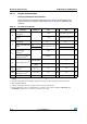
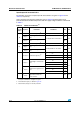
Table 38. TIMx
(1)
characteristics
1. TIMx is used as a general term to refer to the TIM2, TIM3 and TIM4 timers.
Symbol Parameter Conditions Min Max Unit
t
res(TIM)
Timer resolution time
1
t
TIMxCLK
f
TIMxCLK
= 36 MHz
27.8 ns
f
EXT
Timer external clock
frequency on CH1 to CH4
0
f
TIMxCLK
/2
MHz
f
TIMxCLK
= 36 MHz
018MHz
Res
TIM
Timer resolution 16 bit
t
COUNTER
16-bit counter clock period
when internal clock is
selected
1 65536
t
TIMxCLK
f
TIMxCLK
= 36 MHz
0.0278 1820 µs
t
MAX_COUNT
Maximum possible count
65536 × 65536
t
TIMxCLK
f
TIMxCLK
= 36 MHz
119.2 s