
Datasheet

STM32F101x4, STM32F101x6 Electrical characteristics
Doc ID 15058 Rev 5 47/79
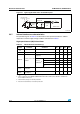
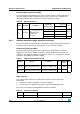
Low-speed internal (LSI) RC oscillator
Wakeup time from low-power mode
The wakeup times given in Tabl e 2 5 are measured on a wakeup phase with an 8-MHz HSI
RC oscillator. The clock source used to wake up the device depends from the current
operating mode:
● Stop or Standby mode: the clock source is the RC oscillator
● Sleep mode: the clock source is the clock that was set before entering Sleep mode.
All timings are derived from tests performed under the ambient temperature and V
DD
supply
voltage conditions summarized in Tabl e 8 .
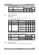
5.3.8 PLL characteristics
The parameters given in Tabl e 2 6 are derived from tests performed under the ambient
temperature and V
DD
supply voltage conditions summarized in Table 8.
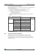
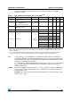
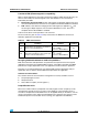
Table 24. LSI oscillator characteristics
(1)
1. V
DD
= 3 V, T
A
= –40 to 85 °C unless otherwise specified.
Symbol Parameter Min Typ Max Unit
f
LSI
(2)
2. Based on characterization, not tested in production.
Frequency 30 40 60 kHz
t
su(LSI)
(3)
3. Guaranteed by design, not tested in production.
LSI oscillator startup time 85 µs
I
DD(LSI)
(3)
LSI oscillator power consumption 0.65 1.2 µA
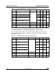
Table 25. Low-power mode wakeup timings
Symbol Parameter Typ Unit
t
WUSLEEP
(1)
1. The wakeup times are measured from the wakeup event to the point at which the user application code
reads the first instruction.
Wakeup from Sleep mode 1.8 µs
t
WUSTOP
(1)
Wakeup from Stop mode (regulator in run mode) 3.6
µs
Wakeup from Stop mode (regulator in low-power mode) 5.4
t
WUSTDBY
(1)
Wakeup from Standby mode 50 µs
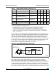
Table 26. PLL characteristics
Symbol Parameter
Value
Unit
Min
(1)
Typ Max
(1)
f
PLL_IN
PLL input clock
(2)
18.025MHz
PLL input clock duty cycle 40 60 %
f
PLL_OUT
PLL multiplier output clock 16 36 MHz