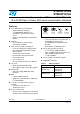
STM32F101x4 STM32F101x6 Low-density access line, ARM-based 32-bit MCU with 16 or 32 KB Flash, 5 timers, ADC and 4 communication interfaces Features ■ Core: ARM 32-bit Cortex™-M3 CPU – 36 MHz maximum frequency, 1.25 DMIPS/MHz (Dhrystone 2.1) performance at 0 wait state memory access – Single-cycle multiplication and hardware division ■ Memories – 16 to 32 Kbytes of Flash memory – 4 to 6 Kbytes of SRAM ■ Clock, reset and supply management – 2.0 to 3.
Contents STM32F101x4, STM32F101x6 Contents 1 Introduction . . . . . . . . . . . . . . . . . . . . . . . . . . . . . . . . . . . . . . . . . . . . . . . . 9 2 Description . . . . . . . . . . . . . . . . . . . . . . . . . . . . . . . . . . . . . . . . . . . . . . . . 10 3 2/79 2.1 Device overview . . . . . . . . . . . . . . . . . . . . . . . . . . . . . . . . . . . . . . . . . . . . 11 2.2 Full compatibility throughout the family . . . . . . . . . . . . . . . . . . . . . . . . . . 14 2.
STM32F101x4, STM32F101x6 Contents 4 Memory mapping . . . . . . . . . . . . . . . . . . . . . . . . . . . . . . . . . . . . . . . . . . 26 5 Electrical characteristics . . . . . . . . . . . . . . . . . . . . . . . . . . . . . . . . . . . . 27 5.1 6 Parameter conditions . . . . . . . . . . . . . . . . . . . . . . . . . . . . . . . . . . . . . . . . 27 5.1.1 Minimum and maximum values . . . . . . . . . . . . . . . . . . . . . . . . . . . . . . . 27 5.1.2 Typical values . . . . . . . . . . . . . . . .
Contents STM32F101x4, STM32F101x6 7 Ordering information scheme . . . . . . . . . . . . . . . . . . . . . . . . . . . . . . . . 76 8 Revision history . . . . . . . . . . . . . . . . . . . . . . . . . . . . . . . . . . . . . . . . . . .
STM32F101x4, STM32F101x6 List of tables List of tables Table 1. Table 2. Table 3. Table 4. Table 5. Table 6. Table 7. Table 8. Table 9. Table 10. Table 11. Table 12. Table 13. Table 14. Table 15. Table 16. Table 17. Table 18. Table 19. Table 20. Table 21. Table 22. Table 23. Table 24. Table 25. Table 26. Table 27. Table 28. Table 29. Table 30. Table 31. Table 32. Table 33. Table 34. Table 35. Table 36. Table 37. Table 38. Table 39. Table 40. Table 41. Table 42. Table 43. Table 44. Device summary . . . .
List of tables Table 45. Table 46. Table 47. Table 48. Table 49. Table 50. Table 51. Table 52. Table 53. 6/79 STM32F101x4, STM32F101x6 ADC accuracy . . . . . . . . . . . . . . . . . . . . . . . . . . . . . . . . . . . . . . . . . . . . . . . . . . . . . . . . . . 66 TS characteristics . . . . . . . . . . . . . . . . . . . . . . . . . . . . . . . . . . . . . . . . . . . . . . . . . . . . . . . . 68 VFQFPN48 7 x 7 mm, 0.5 mm pitch, package mechanical data . . . . . . . . . . . . . . . . . . . .
STM32F101x4, STM32F101x6 List of figures List of figures Figure 1. Figure 2. Figure 3. Figure 4. Figure 5. Figure 6. Figure 7. Figure 8. Figure 9. Figure 10. Figure 11. Figure 12. Figure 13. Figure 14. Figure 15. Figure 16. Figure 17. Figure 18. Figure 19. Figure 20. Figure 21. Figure 22. Figure 23. Figure 24. Figure 25. Figure 26. Figure 27. Figure 28. Figure 29. Figure 30. Figure 31. Figure 32. Figure 33. Figure 34. Figure 35. Figure 36. Figure 37. Figure 38. Figure 39. Figure 40. Figure 41.
List of figures Figure 42. Figure 43. 8/79 STM32F101x4, STM32F101x6 Recommended footprint(1) . . . . . . . . . . . . . . . . . . . . . . . . . . . . . . . . . . . . . . . . . . . . . . . . . 73 LQFP64 PD max vs. TA . . . . . . . . . . . . . . . . . . . . . . . . . . . . . . . . . . . . . . . . . . . . . . . . . . .
STM32F101x4, STM32F101x6 1 Introduction Introduction This datasheet provides the ordering information and mechanical device characteristics of the STM32F101x4 and STM32F101x6 low-density access line microcontrollers. For more details on the whole STMicroelectronics STM32F101xx family, please refer to Section 2.2: Full compatibility throughout the family. The Low-density STM32F101xx datasheet should be read in conjunction with the low-, medium- and high-density STM32F10xxx reference manual.
Description 2 STM32F101x4, STM32F101x6 Description The STM32F101x4 and STM32F101x6 Low-density access line family incorporates the high-performance ARM Cortex™-M3 32-bit RISC core operating at a 36 MHz frequency, high-speed embedded memories (Flash memory of 16 to 32 Kbytes and SRAM of 4 to 6 Kbytes), and an extensive range of enhanced peripherals and I/Os connected to two APB buses.
STM32F101x4, STM32F101x6 Device overview Figure 1 shows the general block diagram of the device family. Table 2. Low-density STM32F101xx device features and peripheral counts Peripheral STM32F101Tx STM32F101Cx STM32F101Rx Flash - Kbytes 16 32 16 32 16 32 SRAM - Kbytes 4 6 4 6 4 6 General-purpose 2 2 2 2 2 2 SPI 1 1 1 1 1 1 I2C 1 1 1 1 1 1 USART 2 2 2 2 2 2 Communication Timers 2.
Description STM32F101x4, STM32F101x6 STM32F101xx Low-density access line block diagram TPIU SW/JTAG Trace/trig SWD Trace controller pbus Ibus Cortex M3 CPU Fmax : 3 6M Hz NVIC Dbus NVIC Syst em AHB: Fmax =36 MHz 7 channels SUPPLY SUPERVISION NRST VDDA VSSA POR / PDR Rst PVD Int @VDD PLL & CLOCK MANAGT XTAL OSC 4-16 MHz PB[ 15:0] GPIOB PC[15:0] GPIOC PD[3:0] GPIOD MOSI,MISO, SCK,NSS as AF OSC_IN OSC_OUT RC 8 MHz IWDG RC 42 kHz Stand by in terface @VDDA VBAT @VBAT RTC AWU AH
STM32F101x4, STM32F101x6 Figure 2. Description Clock tree 8 MHz HSI RC HSI /2 36 MHz max PLLSRC /8 SW PLLMUL HSI ..., x16 x2, x3, x4 PLL SYSCLK PLLCLK AHB Prescaler 36 MHz /1, 2..
Description 2.2 STM32F101x4, STM32F101x6 Full compatibility throughout the family The STM32F101xx is a complete family whose members are fully pin-to-pin, software and feature compatible. In the reference manual, the STM32F101x4 and STM32F101x6 are referred to as low-density devices, the STM32F101x8 and STM32F101xB are referred to as medium-density devices, and the STM32F101xC, STM32F101xD and STM32F101xE are referred to as high-density devices.
STM32F101x4, STM32F101x6 Description 2.3 Overview 2.3.1 ARM® Cortex™-M3 core with embedded Flash and SRAM The ARM Cortex™-M3 processor is the latest generation of ARM processors for embedded systems. It has been developed to provide a low-cost platform that meets the needs of MCU implementation, with a reduced pin count and low-power consumption, while delivering outstanding computational performance and an advanced system response to interrupts.
Description 2.3.6 STM32F101x4, STM32F101x6 External interrupt/event controller (EXTI) The external interrupt/event controller consists of 19 edge detector lines used to generate interrupt/event requests. Each line can be independently configured to select the trigger event (rising edge, falling edge, both) and can be masked independently. A pending register maintains the status of the interrupt requests. The EXTI can detect an external line with a pulse width shorter than the Internal APB2 clock period.
STM32F101x4, STM32F101x6 Description than the VPVD threshold. The interrupt service routine can then generate a warning message and/or put the MCU into a safe state. The PVD is enabled by software. Refer to Table 10: Embedded reset and power control block characteristics for the values of VPOR/PDR and VPVD. 2.3.11 Voltage regulator The regulator has three operation modes: main (MR), low power (LPR) and power down.
Description STM32F101x4, STM32F101x6 Each channel is connected to dedicated hardware DMA requests, with support for software trigger on each channel. Configuration is made by software and transfer sizes between source and destination are independent. The DMA can be used with the main peripherals: SPI, I2C, USART, general purpose timers TIMx and ADC. 2.3.
STM32F101x4, STM32F101x6 Description output compare, PWM or one pulse mode output. This gives up to 12 input captures / output compares / PWMs on the largest packages. The general-purpose timers can work together via the Timer Link feature for synchronization or event chaining. Their counter can be frozen in debug mode. Any of the general-purpose timers can be used to generate PWM outputs. They all have independent DMA request generation.
Description STM32F101x4, STM32F101x6 An analog watchdog feature allows very precise monitoring of the converted voltage of one, some or all selected channels. An interrupt is generated when the converted voltage is outside the programmed thresholds. 2.3.24 Temperature sensor The temperature sensor has to generate a voltage that varies linearly with temperature. The conversion range is between 2 V < VDDA < 3.6 V.
STM32F101x4, STM32F101x6 Pinouts and pin description STM32F101xx Low-density access line LQFP64 pinout VDD_3 VSS_3 PB9 PB8 BOOT0 PB7 PB6 PB5 PB4 PB3 PD2 PC12 PC11 PC10 PA15 PA14 Figure 3.
Pinouts and pin description STM32F101xx Low-density access line VFQPFN48 pinout VDD_3 VSS_3 PB9 PB8 BOOT0 PB7 PB6 PB5 PB4 PB3 PA15 PA14 Figure 5.
STM32F101x4, STM32F101x6 Low-density STM32F101xx pin definitions VFQFPN36 1 1 - 2 2 - 3 3 - Type(1) LQFP64 LQFP48/ VFQFPN48 Pins Pin name VBAT S PC13-TAMPER-RTC(5) I/O PC14-OSC32_IN(5) (5) PC15-OSC32_OUT I/O I/O I / O level(2) Table 4.
Pinouts and pin description Table 4.
STM32F101x4, STM32F101x6 Table 4.
Memory mapping 4 STM32F101x4, STM32F101x6 Memory mapping The memory map is shown in Figure 7. Figure 7.
STM32F101x4, STM32F101x6 Electrical characteristics 5 Electrical characteristics 5.1 Parameter conditions Unless otherwise specified, all voltages are referenced to VSS. 5.1.1 Minimum and maximum values Unless otherwise specified the minimum and maximum values are guaranteed in the worst conditions of ambient temperature, supply voltage and frequencies by tests in production on 100% of the devices with an ambient temperature at TA = 25 °C and TA = TAmax (given by the selected temperature range).
Electrical characteristics Figure 8. STM32F101x4, STM32F101x6 Pin loading conditions Figure 9. Pin input voltage STM32F10xxx pin STM32F10xxx pin C = 50 pF VIN ai14124b ai14123b 5.1.6 Power supply scheme Figure 10. Power supply scheme VBAT Backup circuitry (OSC32K,RTC, Wakeup logic Backup registers) OUT GP I/Os IN Level shifter Po wer swi tch 1.8-3.6V IO Logic Kernel logic (CPU, Digital & Memories) VDD VDD 1/2/3/4/5 5 × 100 nF + 1 × 4.
STM32F101x4, STM32F101x6 5.1.7 Electrical characteristics Current consumption measurement Figure 11. Current consumption measurement scheme IDD_VBAT VBAT IDD VDD VDDA ai14126 5.2 Absolute maximum ratings Stresses above the absolute maximum ratings listed in Table 5: Voltage characteristics, Table 6: Current characteristics, and Table 7: Thermal characteristics may cause permanent damage to the device.
Electrical characteristics Table 6. STM32F101x4, STM32F101x6 Current characteristics Symbol Ratings Max.
STM32F101x4, STM32F101x6 Table 8. Symbol PD Electrical characteristics General operating conditions (continued) Parameter Power dissipation at TA = 85 °C(3) Conditions 444 LQFP48 363 VFQFPN36 1000 Ambient temperature Low power TJ Max LQFP64 Maximum power dissipation TA Min dissipation(4) Junction temperature range Unit mW –40 85 °C –40 105 °C –40 105 °C 1. When the ADC is used, refer to Table 42: ADC characteristics. 2.
Electrical characteristics . Table 10. Embedded reset and power control block characteristics Symbol Parameter Conditions Programmable voltage detector level selection VPVD VPVDhyst STM32F101x4, STM32F101x6 (2) VPOR/PDR VPDRhyst (2) Min Typ Max Unit PLS[2:0]=000 (rising edge) 2.1 2.18 2.26 V PLS[2:0]=000 (falling edge) 2 2.08 2.16 V PLS[2:0]=001 (rising edge) 2.19 2.28 2.37 V PLS[2:0]=001 (falling edge) 2.09 2.18 2.27 V PLS[2:0]=010 (rising edge) 2.28 2.38 2.
STM32F101x4, STM32F101x6 5.3.4 Electrical characteristics Embedded reference voltage The parameters given in Table 11 are derived from tests performed under the ambient temperature and VDD supply voltage conditions summarized in Table 8. Table 11.
Electrical characteristics Table 12. STM32F101x4, STM32F101x6 Maximum current consumption in Run mode, code with data processing running from Flash Max(1) Symbol Parameter Conditions fHCLK Unit TA = 85 °C External clock (2), all peripherals enabled IDD Supply current in Run mode 36 MHz 26 24 MHz 18 16 MHz 13 8 MHz 7 36 MHz 19 24 MHz 13 16 MHz 10 8 MHz 6 mA External clock (2), all peripherals Disabled 1. Based on characterization, not tested in production. 2.
STM32F101x4, STM32F101x6 Electrical characteristics Figure 12. Typical current consumption in Run mode versus frequency (at 3.6 V) code with data processing running from RAM, peripherals enabled 25 Consumption (mA) 20 15 36 MHz 16 MHz 8 MHz 10 5 0 – 45°C 25 °C 70 °C 85 °C Temperature (°C) Figure 13. Typical current consumption in Run mode versus frequency (at 3.
Electrical characteristics Table 14. STM32F101x4, STM32F101x6 Maximum current consumption in Sleep mode, code running from Flash or RAM Max(1) Symbol Parameter Conditions fHCLK Unit TA = 85 °C External clock(2) all peripherals enabled IDD Supply current in Sleep mode 36 MHz 14 24 MHz 10 16 MHz 7 8 MHz 4 36 MHz 5 24 MHz 4.5 16 MHz 4 8 MHz 3 mA External clock(2), all peripherals disabled 1.
STM32F101x4, STM32F101x6 Electrical characteristics Figure 14. Typical current consumption on VBAT with RTC on versus temperature at different VBAT values Consumption ( µA ) 2.5 2 2V 1.5 2.4 V 1 3V 0.5 3.6 V 0 –40 °C 25 °C 70 °C 85 °C 105 °C Temperature (°C) ai17351 Figure 15. Typical current consumption in Stop mode with regulator in Run mode versus temperature at VDD = 3.3 V and 3.6 V 45 40 Consumption (µA) 35 30 25 3.3 V 20 3.
Electrical characteristics STM32F101x4, STM32F101x6 Figure 16. Typical current consumption in Stop mode with regulator in Low-power mode versus temperature at VDD = 3.3 V and 3.6 V 30 Consumption (µA) 25 20 3.3 V 15 3.6 V 10 5 0 –45 °C 25 °C 85 °C Temperature (°C) Figure 17. Typical current consumption in Standby mode versus temperature at VDD = 3.3 V and 3.6 V 3.5 3 Consumption (µA) 2.5 2 3.3 V 3.6 V 1.5 1 0.
STM32F101x4, STM32F101x6 Electrical characteristics Typical current consumption The MCU is placed under the following conditions: ● All I/O pins are in input mode with a static value at VDD or VSS (no load) ● All peripherals are disabled except if it is explicitly mentioned ● The Flash access time is adjusted to fHCLK frequency (0 wait state from 0 to 24 MHz, 1 wait state from 24 to 36 MHz) ● Prefetch is on (reminder: this bit must be set before clock setting and bus prescaling) ● When the periph
Electrical characteristics Table 17. STM32F101x4, STM32F101x6 Typical current consumption in Sleep mode, code running from Flash or RAM Typ(1) Symbol Parameter Conditions (3) External clock IDD Supply current in Sleep mode fHCLK Typ(1) All peripherals All peripherals enabled(2) disabled 36 MHz 6.7 3.1 24 MHz 4.8 2.3 16 MHz 3.4 1.8 8 MHz 2 1.2 4 MHz 1.5 1.1 2 MHz 1.25 1 1 MHz 1.1 0.98 500 kHz 1.05 0.96 125 kHz 1 0.95 36 MHz 6.1 2.5 24 MHz 4.2 1.7 16 MHz 2.8 1.
STM32F101x4, STM32F101x6 Electrical characteristics On-chip peripheral current consumption The current consumption of the on-chip peripherals is given in Table 18.
Electrical characteristics Table 19. STM32F101x4, STM32F101x6 High-speed external user clock characteristics Symbol Parameter Conditions Min Typ Max Unit 1 8 25 MHz fHSE_ext User external clock source frequency(1) VHSEH OSC_IN input pin high level voltage 0.7VDD VDD VHSEL OSC_IN input pin low level voltage VSS 0.
STM32F101x4, STM32F101x6 Electrical characteristics Figure 18. High-speed external clock source AC timing diagram VHSEH 90% VHSEL 10% tr(HSE) tf(HSE) tW(HSE) tW(HSE) t THSE External clock source fHSE_ext OSC _IN IL STM32F10xxx ai14127b Figure 19.
Electrical characteristics Table 21. STM32F101x4, STM32F101x6 HSE 4-16 MHz oscillator characteristics(1)(2) Symbol fOSC_IN Parameter Conditions Min Typ Max Unit 4 8 16 MHz Oscillator frequency RF Feedback resistor 200 kΩ C Recommended load capacitance versus equivalent serial RS = 30 Ω resistance of the crystal (RS)(3) 30 pF i2 HSE driving current VDD = 3.
STM32F101x4, STM32F101x6 Electrical characteristics resonator manufacturer for more details on the resonator characteristics (frequency, package, accuracy). Table 22. Symbol LSE oscillator characteristics (fLSE = 32.768 kHz)(1) (2) Parameter Conditions Min Typ Max RF Feedback resistor C Recommended load capacitance versus equivalent serial resistance of the crystal (RS) RS = 30 KΩ 15 pF I2 LSE driving current VDD = 3.3 V VIN = VSS 1.
Electrical characteristics STM32F101x4, STM32F101x6 Figure 21. Typical application with a 32.768 kHz crystal Resonator with integrated capacitors CL1 fLSE OSC32_IN 32.768 KH z resonator CL2 RF Bias controlled gain STM32F10xxx OSC32_OU T ai14129b 5.3.7 Internal clock source characteristics The parameters given in Table 23 are derived from tests performed under the ambient temperature and VDD supply voltage conditions summarized in Table 8. High-speed internal (HSI) RC oscillator Table 23.
STM32F101x4, STM32F101x6 Electrical characteristics Low-speed internal (LSI) RC oscillator Table 24. LSI oscillator characteristics (1) Symbol fLSI(2) tsu(LSI) Parameter Frequency (3) LSI oscillator startup time (3) LSI oscillator power consumption IDD(LSI) Min Typ Max Unit 30 40 60 kHz 85 µs 1.2 µA 0.65 1. VDD = 3 V, TA = –40 to 85 °C unless otherwise specified. 2. Based on characterization, not tested in production. 3. Guaranteed by design, not tested in production.
Electrical characteristics Table 26. STM32F101x4, STM32F101x6 PLL characteristics Value Symbol Parameter Min(1) Unit Max(1) Typ tLOCK PLL lock time 200 µs Jitter Cycle-to-cycle jitter 300 ps 1. Based on device characterization, not tested in production. 2. Take care of using the appropriate multiplier factors so as to have PLL input clock values compatible with the range defined by fPLL_OUT. 5.3.
STM32F101x4, STM32F101x6 Electrical characteristics Functional EMS (Electromagnetic susceptibility) While a simple application is executed on the device (toggling 2 LEDs through I/O ports). the device is stressed by two electromagnetic events until a failure occurs. The failure is indicated by the LEDs: ● Electrostatic discharge (ESD) (positive and negative) is applied to all device pins until a functional disturbance occurs. This test is compliant with the IEC 61000-4-2 standard.
Electrical characteristics STM32F101x4, STM32F101x6 Electromagnetic Interference (EMI) The electromagnetic field emitted by the device is monitored while a simple application is executed (toggling 2 LEDs through the I/O ports). This emission test is compliant with IEC61967-2 standard which specifies the test board and the pin loading. Table 30. EMI characteristics Symbol Parameter SEMI 5.3.11 Peak level Conditions Monitored frequency band Max vs. [fHSE/fHCLK] Unit 8/36 MHz 0.
STM32F101x4, STM32F101x6 5.3.12 Electrical characteristics I/O current injection characteristics As a general rule, current injection to the I/O pins, due to external voltage below VSS or above VDD (for standard, 3 V-capable I/O pins) should be avoided during normal product operation. However, in order to give an indication of the robustness of the microcontroller in cases when abnormal injection accidentally happens, susceptibility tests are performed on a sample basis during device characterization.
Electrical characteristics 5.3.13 STM32F101x4, STM32F101x6 I/O port characteristics General input/output characteristics Unless otherwise specified, the parameters given in Table 34 are derived from tests performed under the conditions summarized in Table 8. All I/Os are CMOS and TTL compliant. Table 34. Symbol VIL VIH Vhys Ilkg I/O static characteristics Parameter Conditions Min Typ Max Unit Standard IO input low level voltage –0.3 0.28*(VDD-2 V)+0.
STM32F101x4, STM32F101x6 Electrical characteristics All I/Os are CMOS and TTL compliant (no software configuration required). Their characteristics cover more than the strict CMOS-technology or TTL parameters. The coverage of these requirements is shown in Figure 22 and Figure 23 for standard I/Os, and in Figure 24 and Figure 25 for 5 V tolerant I/Os. Figure 22. Standard I/O input characteristics - CMOS port VIH/VIL (V) 1.3 (V -2)+ V IH=0.41 DD 5V D V =0.
Electrical characteristics STM32F101x4, STM32F101x6 Figure 24. 5 V tolerant I/O input characteristics - CMOS port 6)( 6), 6 6 $ 6 $ IREMENTS )( #-/3 6 ), 6 $$ T 6 ), 6 $$ REQUIRMEN /3 STANDARD #- 6 )( 6 $$ REQU STANDARD )NPUT RANGE NOT GUARANTEED 6$$ 6 6$$ AI B Figure 25.
STM32F101x4, STM32F101x6 Electrical characteristics Output driving current The GPIOs (general-purpose inputs/outputs) can sink or source up to ±8 mA, and sink or source up to ±20 mA (with a relaxed VOL/VOH). In the user application, the number of I/O pins which can drive current must be limited to respect the absolute maximum rating specified in Section 5.
Electrical characteristics STM32F101x4, STM32F101x6 Input/output AC characteristics The definition and values of input/output AC characteristics are given in Figure 26 and Table 36, respectively. Unless otherwise specified, the parameters given in Table 36 are derived from tests performed under the ambient temperature and VDD supply voltage conditions summarized in Table 8. Table 36.
STM32F101x4, STM32F101x6 Electrical characteristics Figure 26. I/O AC characteristics definition 90% 10% 50% 50% 90% 10% EXT ERNAL OUTPUT ON 50pF tr(I O)out tr(I O)out T Maximum frequency is achieved if (tr + tf) ≤ 2/3)T and if the duty cycle is (45-55%) when loaded by 50pF ai14131 5.3.14 NRST pin characteristics The NRST pin input driver uses CMOS technology. It is connected to a permanent pull-up resistor, RPU (see Table 34).
Electrical characteristics 5.3.15 STM32F101x4, STM32F101x6 TIM timer characteristics The parameters given in Table 38 are guaranteed by design. Refer to Section 5.3.12: I/O current injection characteristics for details on the input/output alternate function characteristics (output compare, input capture, external clock, PWM output). Table 38. Symbol tres(TIM) fEXT ResTIM tCOUNTER TIMx(1) characteristics Parameter Conditions Min Max 1 tTIMxCLK 27.
STM32F101x4, STM32F101x6 Table 39. Electrical characteristics I2C characteristics Standard mode I2C(1) Fast mode I2C(1)(2) Symbol Parameter Unit Min Max Min Max tw(SCLL) SCL clock low time 4.7 1.3 tw(SCLH) SCL clock high time 4.0 0.6 tsu(SDA) SDA setup time 250 100 (3) 0(4) 900(3) 20+0.1Cb 300 µs th(SDA) SDA data hold time tr(SDA) tr(SCL) SDA and SCL rise time 1000 tf(SDA) tf(SCL) SDA and SCL fall time 300 th(STA) Start condition hold time 4.0 0.
Electrical characteristics STM32F101x4, STM32F101x6 Figure 28. I2C bus AC waveforms and measurement circuit(1) VDD 4 .7 kΩ VDD 4 .7 kΩ 100 Ω 100 Ω I²C bus STM32F10x SDA SCL Start repeated Start Start tsu(STA) SDA tf(SDA) tr(SDA) th(STA) tsu(SDA) tw(SCLL) th(SDA) tsu(STO:STA) Stop SCL tw(SCLH) tr(SCL) tsu(STO) tf(SCL) ai14133d 1. Measurement points are done at CMOS levels: 0.3VDD and 0.7VDD. Table 40. SCL frequency (fPCLK1= MHz, VDD = 3.3 V)(1)(2) I2C_CCR value fSCL (kHz) RP = 4.
STM32F101x4, STM32F101x6 Electrical characteristics SPI interface characteristics Unless otherwise specified, the parameters given in Table 41 are derived from tests performed under the ambient temperature, fPCLKx frequency and VDD supply voltage conditions summarized in Table 8. Refer to Section 5.3.12: I/O current injection characteristics for more details on the input/output alternate function characteristics (NSS, SCK, MOSI, MISO). Table 41.
Electrical characteristics STM32F101x4, STM32F101x6 Figure 29. SPI timing diagram - slave mode and CPHA = 0 NSS input tc(SCK) th(NSS) SCK Input tSU(NSS) CPHA= 0 CPOL=0 tw(SCKH) tw(SCKL) CPHA= 0 CPOL=1 tv(SO) ta(SO) MISO OUT P UT tr(SCK) tf(SCK) th(SO) MS B O UT BI T6 OUT tdis(SO) LSB OUT tsu(SI) MOSI I NPUT B I T1 IN M SB IN LSB IN th(SI) ai14134c Figure 30.
STM32F101x4, STM32F101x6 Electrical characteristics Figure 31. SPI timing diagram - master mode(1) High NSS input SCK Input SCK Input tc(SCK) CPHA= 0 CPOL=0 CPHA= 0 CPOL=1 CPHA=1 CPOL=0 CPHA=1 CPOL=1 tsu(MI) MISO INP UT tw(SCKH) tw(SCKL) MS BIN tr(SCK) tf(SCK) BI T6 IN LSB IN th(MI) MOSI OUTUT M SB OUT tv(MO) B I T1 OUT LSB OUT th(MO) ai14136 1. Measurement points are done at CMOS levels: 0.3VDD and 0.7VDD.
Electrical characteristics 5.3.17 STM32F101x4, STM32F101x6 12-bit ADC characteristics Unless otherwise specified, the parameters given in Table 42 are derived from tests performed under the ambient temperature, fPCLK2 frequency and VDDA supply voltage conditions summarized in Table 8. Note: It is recommended to perform a calibration after each power-up. Table 42. ADC characteristics Symbol Parameter Conditions Min Typ Max Unit VDDA Power supply 2.4 3.6 V fADC ADC clock frequency 0.
STM32F101x4, STM32F101x6 Electrical characteristics Equation 1: RAIN max formula: TS R AIN < ------------------------------------------------------------- – R ADC N+2 f ADC × C ADC × ln ( 2 ) The formula above (Equation 1) is used to determine the maximum external impedance allowed for an error below 1/4 of LSB. Here N = 12 (from 12-bit resolution). Table 43. RAIN max for fADC = 14 MHz(1) Ts (cycles) tS (µs) RAIN max (kΩ) 1.5 0.11 0.4 7.5 0.54 5.9 13.5 0.96 11.4 28.5 2.04 25.2 41.5 2.
Electrical characteristics STM32F101x4, STM32F101x6 ADC accuracy(1) (2) (3) Table 45. Symbol ET Parameter Test conditions Total unadjusted error EO Offset error EG Gain error ED Differential linearity error EL Integral linearity error fPCLK2 = 28 MHz, fADC = 14 MHz, RAIN < 10 kΩ, VDDA = 2.4 V to 3.6 V Measurements made after ADC calibration Typ Max(4) ±2 ±5 ±1.5 ±2.5 ±1.5 ±3 ±1 ±2 ±1.5 ±3 Unit LSB 1. ADC DC accuracy values are measured after internal calibration. 2.
STM32F101x4, STM32F101x6 Electrical characteristics Figure 33. Typical connection diagram using the ADC STM32F10xxx VDD RAIN(1) Sample and hold ADC converter VT 0.6 V RADC(1) AINx VT 0.6 V VAIN Cparasitic 12-bit converter CADC(1) IL±1 µA ai14139d 1. Refer to Table 42 for the values of RAIN, RADC and CADC. 2. Cparasitic represents the capacitance of the PCB (dependent on soldering and PCB layout quality) plus the pad capacitance (roughly 7 pF).
Electrical characteristics 5.3.18 STM32F101x4, STM32F101x6 Temperature sensor characteristics Table 46. TS characteristics Symbol TL(1) Avg_Slope(1) V25(1) tSTART(2) TS_temp(3)(2) Parameter Min VSENSE linearity with temperature Typ Max Unit ±1 ±2 °C Average slope 4.0 4.3 4.6 mV/°C Voltage at 25°C 1.34 1.43 1.52 V 10 µs 17.1 µs Startup time 4 ADC sampling time when reading the temperature 1. Guaranteed by characterization, not tested in production. 2.
STM32F101x4, STM32F101x6 Package characteristics 6 Package characteristics 6.1 Package mechanical data In order to meet environmental requirements, ST offers these devices in different grades of ECOPACK® packages, depending on their level of environmental compliance. ECOPACK® specifications, grade definitions and product status are available at: www.st.com. ECOPACK® is an ST trademark.
Package characteristics STM32F101x4, STM32F101x6 Figure 35. VFQFPN48 7 x 7 mm, 0.5 mm pitch, package Figure 36. Recommended footprint outline(1) (dimensions in mm)(1)(2) ddd C Seating Plane A2 A C 0.75 A1 A3 5.80 37 48 D 36 1 Pin no. 1 ID R = 0.20 e 5.60 37 48 0.20 1 36 5.80 5.60 e 6.20 0.30 E E2 b 6.20 12 25 13 0.55 24 L 0.50 12 25 7.30 ai15799 24 13 L b Bottom View D2 V0_ME 1. Drawing is not to scale. 2.
STM32F101x4, STM32F101x6 Package characteristics Figure 37. VFQFPN36 6 x 6 mm, 0.5 mm pitch, package Figure 38. Recommended footprint outline(1) (dimensions in mm)(1)(2) Seating plane C ddd C A2 A 1.00 4.30 27 A1 A3 19 E2 28 18 b 27 19 0.50 4.10 18 28 4.30 4.10 4.80 4.80 e D2 D 36 10 9 1 0.75 0.30 36 10 6.30 ai14870b Pin # 1 ID R = 0.20 1 9 L E ZR_ME 1. Drawing is not to scale. 2. All leads/pads should also be soldered to the PCB to improve the lead solder joint life.
Package characteristics STM32F101x4, STM32F101x6 Figure 39. LQFP64 – 10 x 10 mm, 64 pin low-profile quad flat package outline(1) Figure 40. Recommended footprint(1)(2) A A2 48 33 A1 0.3 49 E b E1 12.7 32 0.5 10.3 10.3 e 64 17 1.2 1 16 7.8 D1 c L1 D 12.7 ai14909 L ai14398b 1. Drawing is not to scale. 2. Dimensions are in millimeters. Table 49. LQFP64 – 10 x 10 mm, 64-pin low-profile quad flat package mechanical data inches(1) millimeters Symbol Min Typ A Max Min 1.60 A1 0.
STM32F101x4, STM32F101x6 Package characteristics Figure 41. LQFP48 – 7 x 7mm, 48-pin low-profile quad flat package outline(1) Figure 42. Recommended footprint(1)(2) Seating plane C A A2 A1 c b ccc 0.50 1.20 0.25 mm Gage plane C 36 D 0.30 25 37 24 D1 k D3 A1 L 25 36 9.70 0.20 7.30 5.80 L1 7.30 24 37 48 13 12 1 1.20 E3 E1 5.80 E 9.70 ai14911b 48 Pin 1 identification 13 1 12 5B_ME 1. Drawing is not to scale. 2. Dimensions are in millimeters. Table 50.
Package characteristics 6.2 STM32F101x4, STM32F101x6 Thermal characteristics The maximum chip junction temperature (TJmax) must never exceed the values given in Table 8: General operating conditions on page 30.
STM32F101x4, STM32F101x6 Evaluating the maximum junction temperature for an application When ordering the microcontroller, the temperature range is specified in the ordering information scheme shown in Table 52: Ordering information scheme. Each temperature range suffix corresponds to a specific guaranteed ambient temperature at maximum dissipation and, to a specific maximum junction temperature. Here, only temperature range 6 is available (–40 to 85 °C).
Ordering information scheme 7 STM32F101x4, STM32F101x6 Ordering information scheme Table 52. Ordering information scheme Example: STM32 F 101 C 4 T 6 A xxx Device family STM32 = ARM-based 32-bit microcontroller Product type F = general-purpose Device subfamily 101 = access line Pin count T = 36 pins C = 48 pins R = 64 pins Flash memory size 4 = 16 Kbytes of Flash memory 6 = 32 Kbytes of Flash memory Package T = LQFP U = VFQFPN Temperature range 6 = Industrial temperature range, –40 to 85 °C.
STM32F101x4, STM32F101x6 8 Revision history Revision history Table 53. Document revision history Date Revision 23-Sep-2008 1 Initial release. 2 I/O information clarified on page 1. Figure 7: Memory map modified. In Table 4: Low-density STM32F101xx pin definitions: PB4, PB13, PB14, PB15, PB3/TRACESWO moved from Default column to Remap column.
Revision history Table 53. STM32F101x4, STM32F101x6 Document revision history (continued) Date 20-May-2010 19-Apr-2011 78/79 Revision Changes 4 Added VFQFPN48 package. Updated note 2 below Table 39: I2C characteristics Updated Figure 28: I2C bus AC waveforms and measurement circuit(1) Updated Figure 27: Recommended NRST pin protection Updated Section 5.3.
STM32F101x4, STM32F101x6 Please Read Carefully: Information in this document is provided solely in connection with ST products. STMicroelectronics NV and its subsidiaries (“ST”) reserve the right to make changes, corrections, modifications or improvements, to this document, and the products and services described herein at any time, without notice. All ST products are sold pursuant to ST’s terms and conditions of sale.