
Datasheet


STM32F100xC, STM32F100xD, STM32F100xE Electrical characteristics
Doc ID 15081 Rev 7 83/98
Note: Any positive injection current within the limits specified for I
INJ(PIN)
and ΣI
INJ(PIN)
in
Section 5.3.13 does not affect the ADC accuracy.
Figure 33. ADC accuracy characteristics
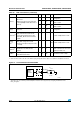
Figure 34. Typical connection diagram using the ADC
1. Refer to Table 51 for the values of R
AIN
, R
ADC
and C
ADC
.
2. C
parasitic
represents the capacitance of the PCB (dependent on soldering and PCB layout quality) plus the
pad capacitance (roughly 7 pF). A high C
parasitic
value will downgrade conversion accuracy. To remedy
this, f
ADC
should be reduced.
General PCB design guidelines
Power supply decoupling should be performed as shown in Figure 35 or Figure 36,
depending on whether V
REF+
is connected to V
DDA
or not. The 10 nF capacitors should be
ceramic (good quality). They should be placed them as close as possible to the chip.
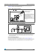
E
O
E
G
1LSB
IDEAL
(1) Example of an actual transfer curve
(2) The ideal transfer curve
(3) End point correlation line
E
T
=Total Unadjusted Error: maximum deviation
between the actual and the ideal transfer curves.
E
O
=Offset Error: deviation between the first actual
transition and the first ideal one.
E
G
=Gain Error: deviation between the last ideal
transition and the last actual one.
E
D
=Differential Linearity Error: maximum deviation
between actual steps and the ideal one.
E
L
=Integral Linearity Error: maximum deviation
between any actual transition and the end point
correlation line.
4095
4094
4093
5
4
3
2
1
0
7
6
1234567
4093 4094 4095 4096
(1)
(2)
E
T
E
D
E
L
(3)
V
DDA
V
SSA
ai14395b
V
REF+
4096
(or depending on package)]
V
DDA
4096
[1LSB
IDEAL
=
ai14139d
STM32F10xxx
V
DD
AINx
I
L
±1 µA
0.6 V
V
T
R
AIN
(1)
C
parasitic
V
AIN
0.6 V
V
T
R
ADC
(1)
C
ADC
(1)
12-bit
converter
Sample and hold ADC
converter