
Datasheet


STM32F100xC, STM32F100xD, STM32F100xE Electrical characteristics
Doc ID 15081 Rev 7 75/98
5.3.16 TIMx characteristics
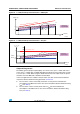
The parameters given in Ta ble 47 are guaranteed by design.
Refer to Section 5.3.13: I/O current injection characteristics for details on the input/output
alternate function characteristics (output compare, input capture, external clock, PWM
output).
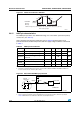
5.3.17 Communications interfaces
I
2
C interface characteristics
Unless otherwise specified, the parameters given in Ta bl e 4 8 are preliminary values derived
from tests performed under the ambient temperature, f
PCLK1
frequency and V
DD
supply
voltage conditions summarized in Ta bl e 9.
The STM32F100xx value line I
2
C interface meets the requirements of the standard I
2
C
communication protocol with the following restrictions: t
he I/O pins SDA and SCL are
mapped to are not “true” open-drain. When configured as open-drain, the PMOS connected
between the I/O pin and V
DD
is disabled, but is still present.
The I
2
C characteristics are described in Ta bl e 4 8. Refer also to
Section 5.3.13: I/O current
injection characteristics
for more details on the input/output alternate function characteristics
(SDA and SCL)
.
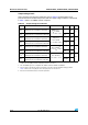
Table 47. TIMx characteristics
Symbol Parameter
Conditions
(1)
1. TIMx is used as a general term to refer to the TIM1, TIM2, TIM3, TIM4, TIM5, TIM15, TIM16 and TIM17
timers.
Min Max Unit
t
res(TIM)
Timer resolution time
1t
TIMxCLK
f
TIMxCLK
= 24 MHz
41.7 ns
f
EXT
Timer external clock
frequency on CHx
(2)
2. CHx is used as a general term to refer to CH1 to CH4 for TIM1, TIM2, TIM3, TIM4 and TIM5, to the CH1 to
CH2 for TIM15, and to CH1 for TIM16 and TIM17.
0f
TIMxCLK
/2 MHz
f
TIMxCLK
= 24 MHz 0 12 MHz
Res
TIM
Timer resolution 16 bit
t
COUNTER
16-bit counter clock period
when the internal clock is
selected
1 65536 t
TIMxCLK
f
TIMxCLK
= 24 MHz
2730 µs
t
MAX_COUNT
Maximum possible count
65536 × 65536 t
TIMxCLK
f
TIMxCLK
= 24 MHz
178 s