
Datasheet


STM32F100xC, STM32F100xD, STM32F100xE Electrical characteristics
Doc ID 15081 Rev 7 71/98
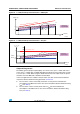
Figure 25. 5 V tolerant I/O input characteristics - CMOS port
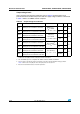
Figure 26. 5 V tolerant I/O input characteristics - TTL port
Output driving current
The GPIOs (general purpose input/outputs) can sink or source up to +/-8 mA, and sink or
source up to +/- 20 mA (with a relaxed VOL/VOH) except PC13, PC14 and PC15 it can sink
or source up to +/-3mA. When using the GPIOs PC13 to PC15 in output mode, the speed
should not exceed 2 MHz with a maximum load of 30 pF.
In the user application, the number of I/O pins which can drive current must be limited to
respect the absolute maximum rating specified in Section 5.2:
● The sum of the currents sourced by all the I/Os on V
DD,
plus the maximum Run
consumption of the MCU sourced on V
DD,
cannot exceed the absolute maximum rating
I
VDD
(see Ta ble 7).
● The sum of the currents sunk by all the I/Os on V
SS
plus the maximum Run
consumption of the MCU sunk on V
SS
cannot exceed the absolute maximum rating
I
VSS
(see Ta bl e 7 ).
9''
&026VWDQGDUGUHTXLUHPHQWV9
,+
9
''
&026VWDQGDUGUHTXLUPHQW9
,/
9
''
9
,+
9
,/
9
9
''
9
,QSXWUDQJH
QRWJXDUDQWHHG
DLE
9
,+
9
''
9
,/
9
''
QRWJXDUDQWHHG
,QSXWUDQJH
77/UHTXLUHPHQW9
,+
9
9
,+
9
''
9
,/
9
''
77/UHTXLUHPHQWV9
,/
9
9
,+
9
,/
9
9
''
9
7
,/PD[
7
,+PLQ
DL