
Datasheet


STM32F100xC, STM32F100xD, STM32F100xE Electrical characteristics
Doc ID 15081 Rev 7 53/98
Wakeup time from low-power mode
The wakeup times given in Tabl e 26 are measured on a wakeup phase with an 8-MHz HSI
RC oscillator. The clock source used to wake up the device depends from the current
operating mode:
● Stop or Standby mode: the clock source is the RC oscillator
● Sleep mode: the clock source is the clock that was set before entering Sleep mode.
All timings are derived from tests performed under the ambient temperature and V
DD
supply
voltage conditions summarized in Ta bl e 9.
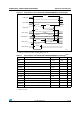
5.3.8 PLL characteristics
The parameters given in Ta ble 27 are derived from tests performed under the ambient
temperature and V
DD
supply voltage conditions summarized in Table 9 .
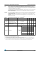
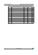
Table 26. Low-power mode wakeup timings
Symbol Parameter Typ Unit
t
WUSLEEP
(1)
1. The wakeup times are measured from the wakeup event to the point at which the user application code
reads the first instruction.
Wakeup from Sleep mode 1.8 µs
t
WUSTOP
(1)
Wakeup from Stop mode (regulator in run mode) 3.6
µs
Wakeup from Stop mode (regulator in low-power mode) 5.4
t
WUSTDBY
(1)
Wakeup from Standby mode 50 µs
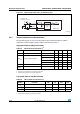
Table 27. PLL characteristics
Symbol Parameter
Value
Unit
Min
(1)
Typ Max
(1)
1. Based on device characterization, not tested in production.
f
PLL_IN
PLL input clock
(2)
2. Take care of using the appropriate multiplier factors so as to have PLL input clock values compatible with
the range defined by f
PLL_OUT
.
18.024MHz
PLL input clock duty cycle 40 60 %
f
PLL_OUT
PLL multiplier output clock 16 24 MHz
t
LOCK
PLL lock time 200 µs
Jitter Cycle-to-cycle jitter 300 ps