
Datasheet


STM32F100xC, STM32F100xD, STM32F100xE Electrical characteristics
Doc ID 15081 Rev 7 47/98
5.3.6 External clock source characteristics
High-speed external user clock generated from an external source
The characteristics given in Tabl e 20 result from tests performed using an high-speed
external clock source, and under the ambient temperature and supply voltage conditions
summarized in Table 9 .
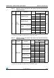
APB2
GPIO A 0.26
mA
GPIO B 0.26
GPIO C 0.26
GPIO D 0.26
GPIO E 0.26
GPIO F 0.24
GPIO G 0.25
ADC1
(3)
1.28
SPI1 0.2
USART1 0.37
TIM1 0.63
TIM15 0.43
TIM16 0.34
TIM17 0.34
1. f
HCLK
= f
APB1
= f
APB2
= 24 MHz, default prescaler value for each peripheral.
2. Specific conditions for DAC: EN1 bit in DAC_CR register set to 1.
3. Specific conditions for ADC: f
HCLK
= 24 MHz, f
APB1
= f
APB2
= f
HCLK
, f
ADCCLK
= f
APB2
/2, ADON bit in the
ADC_CR2 register is set to 1.
Table 19. Peripheral current consumption (continued)
Peripheral Typical consumption at 25 °C
(1)
Unit
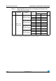
Table 20. High-speed external user clock characteristics
Symbol Parameter Conditions Min Typ Max Unit
f
HSE_ext
User external clock source
frequency
(1)
1824MHz
V
HSEH
OSC_IN input pin high level
voltage
(1)
0.7V
DD
V
DD
V
V
HSEL
OSC_IN input pin low level
voltage
(1)
V
SS
0.3V
DD
t
w(HSE)
t
w(HSE)
OSC_IN high or low time
(1)
5
ns
t
r(HSE)
t
f(HSE)
OSC_IN rise or fall time
(1)
20
C
in(HSE)
OSC_IN input capacitance
(1)
5pF