
Datasheet


STM32F100xC, STM32F100xD, STM32F100xE Electrical characteristics
Doc ID 15081 Rev 7 43/98
Typical current consumption
The MCU is placed under the following conditions:
● All I/O pins are in input mode with a static value at V
DD
or V
SS
(no load)
● All peripherals are disabled except if it is explicitly mentioned
● When the peripherals are enabled f
PCLK1
= f
HCLK
/4, f
PCLK2
= f
HCLK
/2, f
ADCCLK
=
f
PCLK2
/4
The parameters given in Ta ble 17 are derived from tests performed under the ambient
temperature and V
DD
supply voltage conditions summarized in Table 9 .
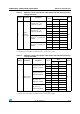
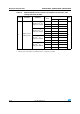
Table 16. Typical and maximum current consumptions in Stop and Standby modes
Symbol Parameter Conditions
Typ
(1)
Max
Unit
V
DD
/V
BAT
= 2.0 V
V
DD
/ V
BAT
= 2.4 V
V
DD
/V
BAT
= 3.3 V
T
A
=
85 °C
T
A
=
105 °C
I
DD
Supply current
in Stop mode
Regulator in Run mode,
Low-speed and high-speed
internal RC oscillators and high-
speed oscillator OFF (no
independent watchdog)
31 320 670
µA
Regulator in Low-Power mode,
Low-speed and high-speed
internal RC oscillators and high-
speed oscillator OFF (no
independent watchdog)
24 305 650
Supply current
in Standby
mode
Low-speed internal RC oscillator
and independent watchdog ON
3.2
Low-speed internal RC oscillator
ON, independent watchdog OFF
3.1
Low-speed internal RC oscillator
and independent watchdog OFF,
low-speed oscillator and RTC
OFF
2.2 3.9 5.7
I
DD_VBAT
Backup
domain supply
current
Low-speed oscillator and RTC
ON
1.0 1.2 1.4 2 2.3
1. Typical values are measured at T
A
= 25 °C.