STM32F100xC STM32F100xD STM32F100xE High-density value line, advanced ARM-based 32-bit MCU with 256 to 512 KB Flash, 16 timers, ADC, DAC & 11 comm interfaces Datasheet −production data Features ■ Core: ARM 32-bit Cortex™-M3 CPU – 24 MHz maximum frequency, 1.25 DMIPS /MHz (Dhrystone 2.1) performance – Single-cycle multiplication and hardware division ■ Memories – 256 to 512 Kbytes of Flash memory – 24 to 32 Kbytes of SRAM – Flexible static memory controller with 4 Chip Selects.
Contents STM32F100xC, STM32F100xD, STM32F100xE Contents 1 Introduction . . . . . . . . . . . . . . . . . . . . . . . . . . . . . . . . . . . . . . . . . . . . . . . . 8 2 Description . . . . . . . . . . . . . . . . . . . . . . . . . . . . . . . . . . . . . . . . . . . . . . . . . 9 3 2/98 2.1 Device overview . . . . . . . . . . . . . . . . . . . . . . . . . . . . . . . . . . . . . . . . . . . . 10 2.2 Overview . . . . . . . . . . . . . . . . . . . . . . . . . . . . . . . . . . . . . . . . . . . .
STM32F100xC, STM32F100xD, STM32F100xE Contents 4 Memory mapping . . . . . . . . . . . . . . . . . . . . . . . . . . . . . . . . . . . . . . . . . . 32 5 Electrical characteristics . . . . . . . . . . . . . . . . . . . . . . . . . . . . . . . . . . . . 34 5.1 6 Parameter conditions . . . . . . . . . . . . . . . . . . . . . . . . . . . . . . . . . . . . . . . . 34 5.1.1 Minimum and maximum values . . . . . . . . . . . . . . . . . . . . . . . . . . . . . . . 34 5.1.2 Typical values . . . . . . . . .
Contents STM32F100xC, STM32F100xD, STM32F100xE 6.2.1 Reference document . . . . . . . . . . . . . . . . . . . . . . . . . . . . . . . . . . . . . . . 92 6.2.2 Selecting the product temperature range . . . . . . . . . . . . . . . . . . . . . . . . 93 7 Ordering information scheme . . . . . . . . . . . . . . . . . . . . . . . . . . . . . . . . 95 8 Revision history . . . . . . . . . . . . . . . . . . . . . . . . . . . . . . . . . . . . . . . . . . .
STM32F100xC, STM32F100xD, STM32F100xE List of tables List of tables Table 1. Table 2. Table 3. Table 4. Table 5. Table 6. Table 7. Table 8. Table 9. Table 10. Table 11. Table 12. Table 13. Table 14. Table 15. Table 16. Table 17. Table 18. Table 19. Table 20. Table 21. Table 22. Table 23. Table 24. Table 25. Table 26. Table 27. Table 28. Table 29. Table 30. Table 31. Table 32. Table 33. Table 34. Table 35. Table 36. Table 37. Table 38. Table 39. Table 40. Table 41. Table 42. Table 43. Table 44.
List of tables Table 45. Table 46. Table 47. Table 48. Table 49. Table 50. Table 51. Table 52. Table 53. Table 54. Table 55. Table 56. Table 57. Table 58. Table 59. Table 60. Table 61. Table 62. 6/98 STM32F100xC, STM32F100xD, STM32F100xE I/O AC characteristics . . . . . . . . . . . . . . . . . . . . . . . . . . . . . . . . . . . . . . . . . . . . . . . . . . . . . 73 NRST pin characteristics . . . . . . . . . . . . . . . . . . . . . . . . . . . . . . . . . . . . . . . . . . . . . . . . . .
STM32F100xC, STM32F100xD, STM32F100xE List of figures List of figures Figure 1. Figure 2. Figure 3. Figure 4. Figure 5. Figure 6. Figure 7. Figure 8. Figure 9. Figure 10. Figure 11. Figure 12. Figure 13. Figure 14. Figure 15. Figure 16. Figure 17. Figure 18. Figure 19. Figure 20. Figure 21. Figure 22. Figure 23. Figure 24. Figure 25. Figure 26. Figure 27. Figure 28. Figure 29. Figure 30. Figure 31. Figure 32. Figure 33. Figure 34. Figure 35. Figure 36. Figure 37. Figure 38. Figure 39. Figure 40.
Introduction 1 STM32F100xC, STM32F100xD, STM32F100xE Introduction This datasheet provides the ordering information and mechanical device characteristics of the STM32F100xC, STM32F100xD and STM32F100xE value line microcontrollers. In the rest of the document, the STM32F100xC, STM32F100xD and STM32F100xE are referred to as high-density value line devices.
STM32F100xC, STM32F100xD, STM32F100xE 2 Description Description The STM32F100xx value line family incorporates the high-performance ARM Cortex™-M3 32-bit RISC core operating at a 24 MHz frequency, high-speed embedded memories (Flash memory up to 512 Kbytes and SRAM up to 32 Kbytes), a flexible static memory control (FSMC) interface (for devices offered in packages of 100 pins and more) and an extensive range of enhanced peripherals and I/Os connected to two APB buses.
Description STM32F100xC, STM32F100xD, STM32F100xE 2.1 Device overview Table 2.
STM32F100xC, STM32F100xD, STM32F100xE STM32F100xx value line block diagram NJTRST JTDI JTCK/SWCLK JTMS/SWDIO JTDO as AF JTAG & SW Ibus Cortex-M3 CPU Fmax : 24 MHz NVIC GP DMA Power VDD18 Voltage reg. 3.3 V to 1.8 V Flash 512 KB 32 bit SRAM 32 KB POR Reset Supply supervision Int POR / PDR @VDDA RC HS @VDDA 12 channels 80 AF EXT.I T WKUP PA[15:0] GPIO port A PB[15:0] GPIO port B @VDD XTAL OSC 4-24 MHz PLL Reset & clock control VSS NRST VDDA VSSA PVD RC LS FSMC VDD= 2.0 V to 3.
Description STM32F100xC, STM32F100xD, STM32F100xE Figure 2. Clock tree )/,7)&/. WR )ODVK SURJUDPPLQJ LQWHUIDFH 0+] +6, 5& +6, 3HULSKHUDO FORFN )60&/. (QDEOH +&/. WR $+% EXV FRUH PHPRU\ DQG '0$ 0+] PD[ 3//65& 6: 3//08/ +6, [ [ [ [ 3// 6<6&/. $+% 3UHVFDOHU 0+] PD[ 3//&/. +6( 0+] $3% 3UHVFDOHU +6( 26& 26& B287 3HULSKHUDO &ORFN (QDEOH /6( 26& N+] WR 57& /6( 3&/.
STM32F100xC, STM32F100xD, STM32F100xE 2.2 Overview 2.2.1 ARM® Cortex™-M3 core with embedded Flash and SRAM Description The ARM Cortex™-M3 processor is the latest generation of ARM processors for embedded systems. It has been developed to provide a low-cost platform that meets the needs of MCU implementation, with a reduced pin count and low-power consumption, while delivering outstanding computational performance and an advanced system response to interrupts.
Description STM32F100xC, STM32F100xD, STM32F100xE specific LCD interfaces. This LCD parallel interface capability makes it easy to build costeffective graphic applications using LCD modules with embedded controllers or highperformance solutions using external controllers with dedicated acceleration. 2.2.
STM32F100xC, STM32F100xD, STM32F100xE Description The boot loader is located in System Memory. It is used to reprogram the Flash memory by using USART1. For further details please refer to AN2606. 2.2.11 2.2.12 Power supply schemes ● VDD = 2.0 to 3.6 V: External power supply for I/Os and the internal regulator. Provided externally through VDD pins. ● VSSA, VDDA = 2.0 to 3.6 V: External analog power supplies for ADC, DAC, Reset blocks, RCs and PLL (minimum voltage to be applied to VDDA is 2.
Description STM32F100xC, STM32F100xD, STM32F100xE either in normal or in low power mode. The device can be woken up from Stop mode by any of the EXTI line. The EXTI line source can be one of the 16 external lines, the PVD output or the RTC alarm. ● Standby mode The Standby mode is used to achieve the lowest power consumption. The internal voltage regulator is switched off so that the entire 1.8 V domain is powered off. The PLL, the HSI RC and the HSE crystal oscillators are also switched off.
STM32F100xC, STM32F100xD, STM32F100xE Table 3.
Description STM32F100xC, STM32F100xD, STM32F100xE TIM2, TIM3, TIM4, TIM5 STM32F100xx devices feature four synchronizable 4-channel general-purpose timers. These timers are based on a 16-bit auto-reload up/downcounter and a 16-bit prescaler. They feature 4 independent channels each for input capture/output compare, PWM or onepulse mode output. This gives up to 12 input captures/output compares/PWMs on the largest packages.
STM32F100xC, STM32F100xD, STM32F100xE Description Window watchdog The window watchdog is based on a 7-bit downcounter that can be set as free running. It can be used as a watchdog to reset the device when a problem occurs. It is clocked from the main clock. It has an early warning interrupt capability and the counter can be frozen in debug mode. SysTick timer This timer is dedicated for OS, but could also be used as a standard down counter. It features: 2.2.
Description STM32F100xC, STM32F100xD, STM32F100xE HDMI (high-definition multimedia interface) consumer electronics control (CEC) The STM32F100xx value line embeds a HDMI-CEC controller that provides hardware support of consumer electronics control (CEC) (Appendix supplement 1 to the HDMI standard). This protocol provides high-level control functions between all audiovisual products in an environment. It is specified to operate at low speeds with minimum processing and memory overhead. 2.2.
STM32F100xC, STM32F100xD, STM32F100xE Description This dual digital Interface supports the following features: ● two DAC converters: one for each output channel ● up to 10-bit output ● left or right data alignment in 12-bit mode ● synchronized update capability ● noise-wave generation ● triangular-wave generation ● dual DAC channels’ independent or simultaneous conversions ● DMA capability for each channel ● external triggers for conversion ● input voltage reference VREF+ Eight DAC tri
Pinouts and pin descriptions STM32F100xC, STM32F100xD, STM32F100xE Pinouts and pin descriptions Figure 3.
STM32F100xC, STM32F100xD, STM32F100xE STM32F100xx value line LQFP100 pinout 100 99 98 97 96 95 94 93 92 91 90 89 88 87 86 85 84 83 82 81 80 79 78 77 76 VDD_3 VSS_3 PE1 PE0 PB9 PB8 BOOT0 PB7 PB6 PB5 PB4 PB3 PD7 PD6 PD5 PD4 PD3 PD2 PD1 PD0 PC12 PC11 PC10 PA15 PA14 Figure 4.
Pinouts and pin descriptions STM32F100xx value line in LQFP64 pinout VDD_3 VSS_3 PB9 PB8 BOOT0 PB7 PB6 PB5 PB4 PB3 PD2 PC12 PC11 PC10 PA15 PA14 Figure 5.
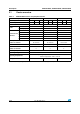
STM32F100xC, STM32F100xD, STM32F100xE High-density STM32F100xx pin definitions (continued) LQFP100 LQFP64 Pin name 15 - - PF5 Type(1) LQFP144 Pins I / O Level(2) Table 4.
Pinouts and pin descriptions High-density STM32F100xx pin definitions (continued) Alternate functions(4) Main function(3) (after reset) Default Remap 40 29 20 PA4 I/O PA4 SPI1_NSS(8)/ USART2_CK(8) DAC_OUT1/ADC_IN4 41 30 21 PA5 I/O PA5 SPI1_SCK(8) DAC_OUT2/ADC_IN5 PA6 SPI1_MISO(8)/ ADC_IN6 / TIM3_CH1(8) TIM1_BKIN / TIM16_CH1 TIM1_CH1N/ TIM17_CH1 42 31 22 26/98 Pin name Type(1) LQFP64 LQFP100 LQFP144 Pins I / O Level(2) Table 4.
STM32F100xC, STM32F100xD, STM32F100xE High-density STM32F100xx pin definitions (continued) Type(1) Alternate functions(4) Main function(3) (after reset) Default Remap LQFP64 LQFP100 LQFP144 Pins I / O Level(2) Table 4.
Pinouts and pin descriptions High-density STM32F100xx pin definitions (continued) Alternate functions(4) LQFP144 LQFP100 LQFP64 Main function(3) (after reset) Pin name 93 - - PG8 94 - - VSS_9 S VSS_9 95 - - VDD_9 S VDD_9 I/O FT Default Remap PG8 96 63 37 PC6 I/O FT PC6 TIM3_CH1 97 64 38 PC7 I/O FT PC7 TIM3_CH2 98 65 39 PC8 I/O FT PC8 TIM13_CH1 TIM3_CH3 99 66 40 PC9 I/O FT PC9 TIM14_CH1 TIM3_CH4 100 67 41 PA8 I/O FT PA8 USART1_CK/ TIM1_CH1(8)/MCO PA9 USA
STM32F100xC, STM32F100xD, STM32F100xE High-density STM32F100xx pin definitions (continued) Type(1) Alternate functions(4) Main function(3) (after reset) Default Remap PD5 FSMC_NWE USART2_TX LQFP64 LQFP100 LQFP144 Pins I / O Level(2) Table 4.
Pinouts and pin descriptions STM32F100xC, STM32F100xD, STM32F100xE 2. FT = 5 V tolerant. 3. Function availability depends on the chosen device. 4. If several peripherals share the same I/O pin, to avoid conflict between these alternate functions only one peripheral should be enabled at a time through the peripheral clock enable bit (in the corresponding RCC peripheral clock enable register). 5. PC13, PC14 and PC15 are supplied through the power switch.
STM32F100xC, STM32F100xD, STM32F100xE Table 5.
Memory mapping STM32F100xC, STM32F100xD, STM32F100xE Table 5. FSMC pin definition (continued) FSMC LQFP100(1) Pins NOR/PSRAM/SRAM NOR/PSRAM Mux PD7 NE1 NE1 Yes PG9 NE2 NE2 - PG10 NE3 NE3 - PG11 - PG12 NE4 NE4 - PG13 A24 A24 - PG14 A25 A25 - PB7 NADV NADV Yes PE0 NBL0 NBL0 Yes PE1 NBL1 NBL1 Yes 1. Ports F and G are not available in devices delivered in 100-pin packages. 4 Memory mapping The memory map is shown in Figure 6.
STM32F100xC, STM32F100xD, STM32F100xE Figure 6.
Electrical characteristics STM32F100xC, STM32F100xD, STM32F100xE 5 Electrical characteristics 5.1 Parameter conditions Unless otherwise specified, all voltages are referenced to VSS. 5.1.
STM32F100xC, STM32F100xD, STM32F100xE Figure 7. Pin loading conditions Electrical characteristics Figure 8. Pin input voltage STM32F10xxx pin STM32F10xxx pin C = 50 pF VIN ai14124b ai14123b 5.1.6 Power supply scheme Figure 9. Power supply scheme 9%$7 %DFNXS FLUFXLWU\ 26& . 57& :DNH XS ORJLF %DFNXS UHJLVWHUV 287 *3 , 2V ,1 /HYHO VKLIWHU 3R ZHU VZL WFK 9 ,2 /RJLF 9'' 9'' î Q) î ) 9'' 5HJXODWRU 966 9''$ 95() Q) ) .
Electrical characteristics 5.1.7 STM32F100xC, STM32F100xD, STM32F100xE Current consumption measurement Figure 10. Current consumption measurement scheme IDD_VBAT VBAT IDD VDD VDDA ai14126 5.2 Absolute maximum ratings Stresses above the absolute maximum ratings listed in Table 6: Voltage characteristics, Table 7: Current characteristics, and Table 8: Thermal characteristics may cause permanent damage to the device.
STM32F100xC, STM32F100xD, STM32F100xE Table 7. Electrical characteristics Current characteristics Symbol Ratings Max.
Electrical characteristics Table 9.
STM32F100xC, STM32F100xD, STM32F100xE 5.3.3 Electrical characteristics Embedded reset and power control block characteristics The parameters given in Table 11 are derived from tests performed under the ambient temperature and VDD supply voltage conditions summarized in Table 9. . Table 11.
Electrical characteristics 5.3.4 STM32F100xC, STM32F100xD, STM32F100xE Embedded reference voltage The parameters given in Table 12 are derived from tests performed under the ambient temperature and VDD supply voltage conditions summarized in Table 9. Table 12. Symbol VREFINT Embedded internal reference voltage Parameter Internal reference voltage Conditions Min Typ Max Unit –40 °C < TA < +105 °C 1.16 1.20 1.26 V –40 °C < TA < +85 °C 1.16 1.20 1.24 V 5.1 17.
STM32F100xC, STM32F100xD, STM32F100xE Table 13. Electrical characteristics Maximum current consumption in Run mode, code with data processing running from Flash Max(1) Symbol Parameter Conditions External clock (2), all peripherals enabled External clock(2), all peripherals disabled IDD Supply current in Run mode fHCLK Unit TA = 85 °C TA = 105 °C 24 MHz 19.7 20 16 MHz 14.6 14.7 8 MHz 8.2 8.6 24 MHz 11.3 11.6 16 MHz 8.7 8.9 8 MHz 5.6 6 24 MHz 19 19 16 MHz 13.1 13.
Electrical characteristics Table 15. STM32F100xC, STM32F100xD, STM32F100xE STM32F100xxB maximum current consumption in Sleep mode, code running from Flash or RAM Max(1) Symbol Parameter Conditions External clock(2) all peripherals enabled External clock(2), all peripherals disabled IDD Supply current in Sleep mode fHCLK Unit TA = 85 °C TA = 105 °C 24 MHz 14.1 14.3 16 MHz 9.7 10.3 8 MHz 5.9 6.2 24 MHz 4.2 4.6 16 MHz 3.7 4.1 8 MHz 2.9 3.4 24 MHz 12.5 12.7 16 MHz 8.2 8.
STM32F100xC, STM32F100xD, STM32F100xE Table 16. Electrical characteristics Typical and maximum current consumptions in Stop and Standby modes Typ(1) Symbol Parameter Conditions VDD/VBAT VDD/ VBAT VDD/VBAT TA = TA = = 2.0 V = 2.4 V = 3.
Electrical characteristics Table 17. STM32F100xC, STM32F100xD, STM32F100xE Typical current consumption in Run mode, code with data processing running from Flash Typical values(1) Symbol Parameter Conditions Running on high-speed external clock with an 8 MHz crystal(3) IDD Supply current in Run mode fHCLK All peripherals All peripherals enabled(2) disabled 24 MHz 14.1 9.5 16 MHz 10 6.85 8 MHz 5.8 4.05 4 MHz 3.6 2.65 2 MHz 2.3 1.85 1 MHz 1.7 1.46 500 kHz 1.4 1.3 125 kHz 1.
STM32F100xC, STM32F100xD, STM32F100xE Table 18. Electrical characteristics Typical current consumption in Sleep mode, code running from Flash or RAM Typical values(1) Symbol Parameter Conditions Running on high-speed external clock with an 8 MHz crystal(3) IDD Supply current in Sleep mode fHCLK All peripherals All peripherals enabled(2) disabled 24 MHz 8.7 2.75 16 MHz 6.1 2.1 8 MHz 3.3 1.3 4 MHz 2.25 1.2 2 MHz 1.65 1.15 1 MHz 1.35 1.1 500 kHz 1.2 1.07 125 kHz 1.1 1.
Electrical characteristics STM32F100xC, STM32F100xD, STM32F100xE On-chip peripheral current consumption The current consumption of the on-chip peripherals is given in Table 19.
STM32F100xC, STM32F100xD, STM32F100xE Table 19. Electrical characteristics Peripheral current consumption (continued) Peripheral Typical consumption at 25 °C(1) GPIO A 0.26 GPIO B 0.26 GPIO C 0.26 GPIO D 0.26 GPIO E 0.26 GPIO F 0.24 GPIO G 0.25 (3) 1.28 APB2 ADC1 Unit mA SPI1 0.2 USART1 0.37 TIM1 0.63 TIM15 0.43 TIM16 0.34 TIM17 0.34 1. fHCLK = fAPB1 = fAPB2 = 24 MHz, default prescaler value for each peripheral. 2.
Electrical characteristics Table 20. STM32F100xC, STM32F100xD, STM32F100xE High-speed external user clock characteristics Symbol Parameter Conditions Min (1) DuCy(HSE) Duty cycle IL Typ 45 OSC_IN Input leakage current VSS ≤VIN ≤VDD Max Unit 55 % ±1 µA 1. Guaranteed by design, not tested in production.
STM32F100xC, STM32F100xD, STM32F100xE Electrical characteristics Figure 11. High-speed external clock source AC timing diagram VHSEH 90% VHSEL 10% tr(HSE) tf(HSE) tW(HSE) tW(HSE) t THSE External clock source fHSE_ext OSC _IN IL STM32F10xxx ai14127b Figure 12.
Electrical characteristics Table 22. STM32F100xC, STM32F100xD, STM32F100xE HSE 4-24 MHz oscillator characteristics(1)(2) Symbol fOSC_IN RF Parameter Conditions Oscillator frequency RS = 30 Ω i2 HSE driving current VDD = 3.
STM32F100xC, STM32F100xD, STM32F100xE Electrical characteristics Note: For CL1 and CL2 it is recommended to use high-quality ceramic capacitors in the 5 pF to 15 pF range selected to match the requirements of the crystal or resonator. CL1 and CL2, are usually the same size. The crystal manufacturer typically specifies a load capacitance which is the series combination of CL1 and CL2.
Electrical characteristics STM32F100xC, STM32F100xD, STM32F100xE Figure 14. Typical application with a 32.768 kHz crystal Resonator with integrated capacitors CL1 fLSE OSC32_IN 32.768 KH z resonator RF Bias controlled gain STM32F10xxx OSC32_OU T CL2 ai14129b 5.3.7 Internal clock source characteristics The parameters given in Table 24 are derived from tests performed under the ambient temperature and VDD supply voltage conditions summarized in Table 9.
STM32F100xC, STM32F100xD, STM32F100xE Electrical characteristics Wakeup time from low-power mode The wakeup times given in Table 26 are measured on a wakeup phase with an 8-MHz HSI RC oscillator. The clock source used to wake up the device depends from the current operating mode: ● Stop or Standby mode: the clock source is the RC oscillator ● Sleep mode: the clock source is the clock that was set before entering Sleep mode.
Electrical characteristics 5.3.9 STM32F100xC, STM32F100xD, STM32F100xE Memory characteristics Flash memory The characteristics are given at TA = –40 to 105 °C unless otherwise specified. Table 28. Flash memory characteristics Symbol Parameter Conditions Min(1) Typ Max(1) Unit tprog 16-bit programming time TA = –40 to +105 °C 40 52.5 70 µs tERASE Page (2 KB) erase time TA = –40 to +105 °C 20 40 ms Mass erase time TA = –40 to +105 °C 20 40 ms Read mode fHCLK = 24 MHz, VDD = 3.
STM32F100xC, STM32F100xD, STM32F100xE Electrical characteristics Figure 15. Asynchronous non-multiplexed SRAM/PSRAM/NOR read waveforms )60&B1( W Y 12(B1( W Z 12( W K 1(B12( )60&B12( )60&B1:( WY $B1( )60&B$> @ W K $B12( $GGUHVV WY %/B1( W K %/B12( )60&B1%/> @ W K 'DWDB1( W VX 'DWDB12( WK 'DWDB12( W VX 'DWDB1( 'DWD )60&B'> @ W Y 1$'9B1( WZ 1$'9 )60&B1$'9 06 9 1. Mode 2/B, C and D only. In Mode 1, FSMC_NADV is not used.
Electrical characteristics Table 30. STM32F100xC, STM32F100xD, STM32F100xE Asynchronous non-multiplexed SRAM/PSRAM/NOR read timings(1) (2) Symbol Parameter Max Unit tw(NE) FSMC_NE low time 5THCLK – 1.5 5THCLK + 2 ns tv(NOE_NE) FSMC_NEx low to FSMC_NOE low 0.5 1.5 ns tw(NOE) FSMC_NOE low time 5THCLK – 1.5 5THCLK + 1.5 ns th(NE_NOE) FSMC_NOE high to FSMC_NE high hold time –1.
STM32F100xC, STM32F100xD, STM32F100xE Electrical characteristics Figure 16. Asynchronous non-multiplexed SRAM/PSRAM/NOR write waveforms tw(NE) FSMC_NEx FSMC_NOE tv(NWE_NE) tw(NWE) t h(NE_NWE) FSMC_NWE tv(A_NE) FSMC_A[25:0] th(A_NWE) Address tv(BL_NE) FSMC_NBL[1:0] th(BL_NWE) NBL tv(Data_NE) th(Data_NWE) Data FSMC_D[15:0] t v(NADV_NE) tw(NADV) FSMC_NADV(1) ai14990 1. Mode 2/B, C and D only. In Mode 1, FSMC_NADV is not used. Table 31.
Electrical characteristics STM32F100xC, STM32F100xD, STM32F100xE Figure 17. Asynchronous multiplexed PSRAM/NOR read waveforms tw(NE) FSMC_NE tv(NOE_NE) t h(NE_NOE) FSMC_NOE t w(NOE) FSMC_NWE tv(A_NE) FSMC_A[25:16] t h(A_NOE) Address tv(BL_NE) th(BL_NOE) FSMC_NBL[1:0] NBL th(Data_NE) tsu(Data_NE) t v(A_NE) tsu(Data_NOE) Address FSMC_AD[15:0] t v(NADV_NE) th(Data_NOE) Data th(AD_NADV) tw(NADV) FSMC_NADV ai14892b Table 32.
STM32F100xC, STM32F100xD, STM32F100xE Electrical characteristics Figure 18. Asynchronous multiplexed PSRAM/NOR write waveforms tw(NE) FSMC_NEx FSMC_NOE tv(NWE_NE) tw(NWE) t h(NE_NWE) FSMC_NWE tv(A_NE) FSMC_A[25:16] th(A_NWE) Address tv(BL_NE) th(BL_NWE) FSMC_NBL[1:0] NBL t v(A_NE) t v(Data_NADV) Address FSMC_AD[15:0] t v(NADV_NE) th(Data_NWE) Data th(AD_NADV) tw(NADV) FSMC_NADV ai14891B Table 33.
Electrical characteristics STM32F100xC, STM32F100xD, STM32F100xE Synchronous waveforms and timings Figure 19 through Figure 22 represent synchronous waveforms and Table 35 through Table 37 provide the corresponding timings.
STM32F100xC, STM32F100xD, STM32F100xE Table 34. Electrical characteristics Synchronous multiplexed NOR/PSRAM read timings(1)(2) Symbol Parameter Min Max Unit tw(CLK) FSMC_CLK period td(CLKL-NExL) FSMC_CLK low to FSMC_NEx low (x = 0...2) td(CLKL-NExH) FSMC_CLK low to FSMC_NEx high (x = 0...2) td(CLKL-NADVL) FSMC_CLK low to FSMC_NADV low td(CLKL-NADVH) FSMC_CLK low to FSMC_NADV high td(CLKL-AV) FSMC_CLK low to FSMC_Ax valid (x = 16...
Electrical characteristics STM32F100xC, STM32F100xD, STM32F100xE Figure 20. Synchronous multiplexed PSRAM write timings %867851 WZ &/. WZ &/. )60&B&/. 'DWD ODWHQF\ WG &/./ 1([/ WG &/./ 1([+ )60&B1([ WG &/./ 1$'9/ WG &/./ 1$'9+ )60&B1$'9 WG &/./ $9 WG &/./ $,9 )60&B$> @ WG &/./ 1:(/ WG &/./ 1:(+ )60&B1:( WG &/./ $',9 WG &/./ $'9 )60&B$'> @ WG &/./ 'DWD WG &/./ 'DWD $'> @ ' ' )60&B1:$,7 :$,7&)* E :$,732/ E WVX 1:$,79 &/.+ WK &/.+ 1:$,79 WG &/.
STM32F100xC, STM32F100xD, STM32F100xE Table 35. Electrical characteristics Synchronous multiplexed PSRAM write timings(1)(2) Symbol Parameter Min Max Unit tw(CLK) FSMC_CLK period td(CLKL-NExL) FSMC_CLK low to FSMC_Nex low (x = 0...2) td(CLKL-NExH) FSMC_CLK low to FSMC_NEx high (x = 0...2) td(CLKL-NADVL) FSMC_CLK low to FSMC_NADV low td(CLKL-NADVH) FSMC_CLK low to FSMC_NADV high td(CLKL-AV) FSMC_CLK low to FSMC_Ax valid (x = 16...25) td(CLKL-AIV) FSMC_CLK low to FSMC_Ax invalid (x = 16..
Electrical characteristics STM32F100xC, STM32F100xD, STM32F100xE Figure 21. Synchronous non-multiplexed NOR/PSRAM read timings %867851 WZ &/. WZ &/. )60&B&/. WG &/./ 1([/ WG &/./ 1([+ 'DWD ODWHQF\ )60&B1([ WG &/./ 1$'9/ WG &/./ 1$'9+ )60&B1$'9 WG &/./ $,9 WG &/./ $9 )60&B$> @ WG &/.+ 12(/ WG &/./ 12(+ )60&B12( WVX '9 &/.+ WK &/.+ '9 WVX '9 &/.+ )60&B'> @ WK &/.+ '9 ' WVX 1:$,79 &/.+ ' ' WK &/.+ 1:$,79 )60&B1:$,7 :$,7&)* E :$,732/ E WVX 1:$,79 &/.+ W K &/.
STM32F100xC, STM32F100xD, STM32F100xE Electrical characteristics Figure 22. Synchronous non-multiplexed PSRAM write timings WZ &/. %867851 WZ &/. )60&B&/. WG &/./ 1([/ WG &/./ 1([+ 'DWD ODWHQF\ )60&B1([ WG &/./ 1$'9/ WG &/./ 1$'9+ )60&B1$'9 WG &/./ $9 WG &/./ $,9 )60&B$> @ WG &/./ 1:(/ WG &/./ 1:(+ )60&B1:( WG &/./ 'DWD )60&B'> @ WG &/./ 'DWD ' ' )60&B1:$,7 :$,7&)* E :$,732/ E WVX 1:$,79 &/.+ WG &/./ 1%/+ WK &/.+ 1:$,79 )60&B1%/ DL L Table 37.
Electrical characteristics 5.3.11 STM32F100xC, STM32F100xD, STM32F100xE EMC characteristics Susceptibility tests are performed on a sample basis during device characterization. Functional EMS (Electromagnetic susceptibility) While a simple application is executed on the device (toggling 2 LEDs through I/O ports). the device is stressed by two electromagnetic events until a failure occurs.
STM32F100xC, STM32F100xD, STM32F100xE Electrical characteristics Electromagnetic Interference (EMI) The electromagnetic field emitted by the device is monitored while a simple application is executed (toggling 2 LEDs through the I/O ports). This emission test is compliant with IEC 61967-2 standard which specifies the test board and the pin loading. Table 39. EMI characteristics Symbol Parameter SEMI 5.3.12 Peak level Monitored frequency band Conditions VDD = 3.
Electrical characteristics 5.3.13 STM32F100xC, STM32F100xD, STM32F100xE I/O current injection characteristics As a general rule, current injection to the I/O pins, due to external voltage below VSS or above VDD (for standard, 3 V-capable I/O pins) should be avoided during normal product operation.
STM32F100xC, STM32F100xD, STM32F100xE 5.3.14 Electrical characteristics I/O port characteristics General input/output characteristics Unless otherwise specified, the parameters given in Table 43 are derived from tests performed under the conditions summarized in Table 9. All I/Os are CMOS and TTL compliant. Table 43. Symbol VIL VIH Vhys Ilkg I/O static characteristics Parameter Conditions Min Typ Max Standard I/O input low level voltage –0.3 0.28*(VDD–2 V)+0.
Electrical characteristics STM32F100xC, STM32F100xD, STM32F100xE Figure 23. Standard I/O input characteristics - CMOS port 9,+ 9,/ 9 PHQW 9 ,+ TXLUH QGDUG UH WD &026 V 7,+PLQ 7,/PD[ 9 9 ,+ '' 9 '' LUHPHQW 9 ,/ UG UHTX &026 VWDQGD ,QSXW UDQJH QRW JXDUDQWHHG 9 9,/ '' 9 '' 9'' 9 DL E Figure 24.
STM32F100xC, STM32F100xD, STM32F100xE Electrical characteristics Figure 25. 5 V tolerant I/O input characteristics - CMOS port 9,+ 9,/ 9 WV 9 ,+ XLUHPHQ UHT WDQGDUG &026 V ,QSXW UDQJH QRW JXDUDQWHHG 9 ,/ 9 '' W 9 ,/ 9 '' UHTXLUPHQ 26 VWDQGDUG &0 9 ,+ 9 '' 9 '' 9'' 9 9'' DL E Figure 26.
Electrical characteristics STM32F100xC, STM32F100xD, STM32F100xE Output voltage levels Unless otherwise specified, the parameters given in Table 44 are derived from tests performed under the ambient temperature and VDD supply voltage conditions summarized in Table 9. All I/Os are CMOS and TTL compliant. Table 44.
STM32F100xC, STM32F100xD, STM32F100xE Electrical characteristics Input/output AC characteristics The definition and values of input/output AC characteristics are given in Figure 27 and Table 45, respectively. Unless otherwise specified, the parameters given in Table 45 are derived from tests performed under the ambient temperature and VDD supply voltage conditions summarized in Table 9. Table 45.
Electrical characteristics STM32F100xC, STM32F100xD, STM32F100xE Figure 27. I/O AC characteristics definition 90% 10% 50% 50% 90% 10% tr(I O)out EXT ERNAL OUTPUT ON 50pF tr(I O)out T Maximum frequency is achieved if (tr + tf) 2/3)T and if the duty cycle is (45-55%) when loaded by 50pF ai14131 5.3.15 NRST pin characteristics The NRST pin input driver uses CMOS technology. It is connected to a permanent pull-up resistor, RPU (see Table 43).
STM32F100xC, STM32F100xD, STM32F100xE 5.3.16 Electrical characteristics TIMx characteristics The parameters given in Table 47 are guaranteed by design. Refer to Section 5.3.13: I/O current injection characteristics for details on the input/output alternate function characteristics (output compare, input capture, external clock, PWM output). Table 47.
Electrical characteristics Table 48. STM32F100xC, STM32F100xD, STM32F100xE I2C characteristics Standard mode I2C(1) Fast mode I2C(1)(2) Symbol Parameter Unit Min Max Min Max tw(SCLL) SCL clock low time 4.7 1.3 tw(SCLH) SCL clock high time 4.0 0.6 tsu(SDA) SDA setup time 250 100 th(SDA) SDA data hold time 0 0 tr(SDA) tr(SCL) SDA and SCL rise time 1000 300 tf(SDA) tf(SCL) SDA and SCL fall time 300 300 th(STA) Start condition hold time 4.0 0.
STM32F100xC, STM32F100xD, STM32F100xE Electrical characteristics Figure 29. I2C bus AC waveforms and measurement circuit 9'' N! 9'' N! ! ! ,ð& EXV 670 ) [ 6'$ 6&/ 6WDUW UHSHDWHG 6WDUW 6WDUW WVX 67$ 6'$ WI 6'$ WU 6'$ WK 67$ WVX 6'$ WZ 6&// 6&/ WZ 6&/+ WU 6&/ WVX 672 67$ 6WRS WK 6'$ WVX 672 WI 6&/ DL G 1. Measurement points are done at CMOS levels: 0.3VDD and 0.7VDD. Table 49. SCL frequency (fPCLK1= 24 MHz, VDD = 3.3 V)(1)(2) I2C_CCR value fSCL (kHz)(3) RP = 4.
Electrical characteristics STM32F100xC, STM32F100xD, STM32F100xE SPI interface characteristics Unless otherwise specified, the parameters given in Table 50 are preliminary values derived from tests performed under the ambient temperature, fPCLKx frequency and VDD supply voltage conditions summarized in Table 9. Refer to Section 5.3.13: I/O current injection characteristics for more details on the input/output alternate function characteristics (NSS, SCK, MOSI, MISO). Table 50.
STM32F100xC, STM32F100xD, STM32F100xE Electrical characteristics Figure 30. SPI timing diagram - slave mode and CPHA = 0 NSS input tc(SCK) th(NSS) SCK Input tSU(NSS) CPHA= 0 CPOL=0 tw(SCKH) tw(SCKL) CPHA= 0 CPOL=1 tv(SO) ta(SO) MISO OUT P UT tr(SCK) tf(SCK) th(SO) MS B O UT BI T6 OUT tdis(SO) LSB OUT tsu(SI) MOSI I NPUT B I T1 IN M SB IN LSB IN th(SI) ai14134c Figure 31.
Electrical characteristics STM32F100xC, STM32F100xD, STM32F100xE Figure 32. SPI timing diagram - master mode High NSS input SCK output SCK output tc(SCK) CPHA= 0 CPOL=0 CPHA= 0 CPOL=1 CPHA=1 CPOL=0 CPHA=1 CPOL=1 tsu(MI) MISO INP UT tw(SCKH) tw(SCKL) tr(SCK) tf(SCK) MS BIN BI T6 IN LSB IN th(MI) MOSI OUTUT M SB OUT B I T1 OUT tv(MO) LSB OUT th(MO) ai14136 1. Measurement points are done at CMOS levels: 0.3VDD and 0.7VDD. HDMI consumer electronics control (CEC) Refer to Section 5.3.
STM32F100xC, STM32F100xD, STM32F100xE Table 51. ADC characteristics Symbol Parameter Conditions Electrical characteristics Min Typ Max Unit VDDA Power supply 2.4 3.6 V VREF+ Positive reference voltage 2.4 VDDA V IVREF Current on the VREF input pin 220(1) µA fADC ADC clock frequency 0.6 12 MHz fS(2) Sampling rate 0.
Electrical characteristics Table 52. STM32F100xC, STM32F100xD, STM32F100xE RAIN max for fADC = 12 MHz(1) Ts (cycles) tS (µs) RAIN max (kΩ) 1.5 0.125 0.4 7.5 0.625 5.9 13.5 1.125 11.4 28.5 2.375 25.2 41.5 3.45 37.2 55.5 4.625 50 71.5 5.96 NA 239.5 20 NA 1. Guaranteed by design, not tested in production. Table 53.
STM32F100xC, STM32F100xD, STM32F100xE Note: Electrical characteristics Any positive injection current within the limits specified for IINJ(PIN) and ΣIINJ(PIN) in Section 5.3.13 does not affect the ADC accuracy. Figure 33.
Electrical characteristics STM32F100xC, STM32F100xD, STM32F100xE Figure 35. Power supply and reference decoupling (VREF+ not connected to VDDA) STM32F10xxx V REF+ 1 µF // 10 nF V DDA 1 µF // 10 nF V SSA/V REF- ai14380b 1. VREF+ is available on 100-pin packages and on TFBGA64 packages. VREF- is available on 100-pin packages only. Figure 36. Power supply and reference decoupling (VREF+ connected to VDDA) STM32F10xxx VREF+/VDDA 1 µF // 10 nF VREF–/VSSA ai14381b 1.
STM32F100xC, STM32F100xD, STM32F100xE Electrical characteristics 5.3.19 DAC electrical specifications Table 55. DAC characteristics Symbol Parameter Min Typ Max(1) Unit VDDA Analog supply voltage 2.4 3.6 V VREF+ Reference supply voltage 2.4 3.
Electrical characteristics Table 55.
STM32F100xC, STM32F100xD, STM32F100xE 5.3.20 Temperature sensor characteristics Table 56. TS characteristics Symbol TL(1) Parameter Electrical characteristics Min VSENSE linearity with temperature (1) Typ Max Unit ±1 ±2 °C Average slope 4.0 4.3 4.6 mV/°C V25(1) Voltage at 25°C 1.32 1.41 1.50 V tSTART(2) Startup time 10 µs TS_temp(3)(2) ADC sampling time when reading the temperature 17.1 µs Avg_Slope 4 1. Guaranteed by characterization, not tested in production. 2.
Package characteristics STM32F100xC, STM32F100xD, STM32F100xE 6 Package characteristics 6.1 Package mechanical data In order to meet environmental requirements, ST offers these devices in different grades of ECOPACK® packages, depending on their level of environmental compliance. ECOPACK® specifications, grade definitions and product status are available at: www.st.com. ECOPACK® is an ST trademark.
STM32F100xC, STM32F100xD, STM32F100xE Package characteristics Figure 38. LQFP144, 20 x 20 mm, 144-pin thin quad flat package outline Figure 39. Recommended footprint Seating plane C A A2 A1 c b ccc 0.25 mm gage plane C D 108 109 k 1.35 73 72 0.35 D1 A1 D3 108 73 L 0.5 L1 17.85 72 109 19.9 E1 144 E E3 22.6 37 1 36 19.9 22.6 ai14 144 Pin 1 identification 37 36 1 e ME_1A 1. Drawing is not to scale. 2. Dimensions are in millimeters. Table 57.
Package characteristics STM32F100xC, STM32F100xD, STM32F100xE Figure 40. LQFP100 – 14 x 14 mm, 100-pin low-profile Figure 41. Recommended footprint quad flat package outline 0.25 mm 0.10 inch GAGE PLANE 75 k 51 D 76 L D1 50 0.5 L1 D3 51 75 C 0.3 76 50 16.7 14.3 b E3 E1 E 100 26 1.2 100 1 26 Pin 1 1 identification 25 12.3 C ccc 25 16.7 e A1 ai14906b A2 A SEATING PLANE C 1L_ME 1. Drawing is not to scale. 2. Dimensions are in millimeters. Table 58.
STM32F100xC, STM32F100xD, STM32F100xE Package characteristics Figure 42. LQFP64 – 10 x 10 mm, 64 pin low-profile quad Figure 43. Recommended flat package outline footprint A A2 48 A1 33 0.3 49 E 32 0.5 b E1 12.7 10.3 10.3 e 64 17 1.2 1 16 7.8 D1 c 12.7 L1 D ai14909 L ai14398b 1. Drawing is not to scale. 2. Dimensions are in millimeters. Table 59. LQFP64 – 10 x 10 mm, 64 pin low-profile quad flat package mechanical data inches(1) millimeters Symbol Min Typ A Max Min Typ 1.
Package characteristics 6.2 STM32F100xC, STM32F100xD, STM32F100xE Thermal characteristics The maximum chip junction temperature (TJmax) must never exceed the values given in Table 9: General operating conditions on page 37.
STM32F100xC, STM32F100xD, STM32F100xE 6.2.2 Package characteristics Selecting the product temperature range When ordering the microcontroller, the temperature range is specified in the ordering information scheme shown in Table 61: Ordering information scheme. Each temperature range suffix corresponds to a specific guaranteed ambient temperature at maximum dissipation and, to a specific maximum junction temperature.
Package characteristics STM32F100xC, STM32F100xD, STM32F100xE Using the values obtained in Table 60 TJmax is calculated as follows: – For LQFP100, 40 °C/W TJmax = 115 °C + (40 °C/W × 134 mW) = 115 °C + 5.4 °C = 120.4 °C This is within the range of the suffix 7 version parts (–40 < TJ < 125 °C). In this case, parts must be ordered at least with the temperature range suffix 7 (see Table 61: Ordering information scheme). Figure 44. LQFP100 PD max vs.
STM32F100xC, STM32F100xD, STM32F100xE 7 Ordering information scheme Ordering information scheme Table 61.
Revision history 8 STM32F100xC, STM32F100xD, STM32F100xE Revision history Table 62. Document revision history Date Revision 09-Oct-2008 1 Initial release. 31-Mar-2009 2 I/O information clarified on page 1. Table 5: High-density STM32F100xx pin definitions modified. Figure 5: Memory map on page 26 modified.
STM32F100xC, STM32F100xD, STM32F100xE Table 62. Revision history Document revision history (continued) Date 08-Jun-2012 17-Sep-2012 Revision Changes 6 Updated Table 7: Current characteristics on page 37 Corrected “CLKL-NOEL” in Section 5.3.10: FSMC characteristics on page 54 Updated Table 48: I2C characteristics on page 76 Corrected note “non-robust “ in Section 5.3.18: 12-bit ADC characteristics on page 80 Updated Figure 1: STM32F100xx value line block diagram on page 11 Updated Section 5.3.
STM32F100xC, STM32F100xD, STM32F100xE Please Read Carefully: Information in this document is provided solely in connection with ST products. STMicroelectronics NV and its subsidiaries (“ST”) reserve the right to make changes, corrections, modifications or improvements, to this document, and the products and services described herein at any time, without notice. All ST products are sold pursuant to ST’s terms and conditions of sale.