
Datasheet

STM32F100x4, STM32F100x6, STM32F100x8, STM32F100xB Electrical characteristics
Doc ID 16455 Rev 7 73/88
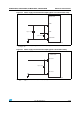
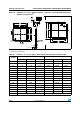
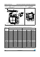
Figure 36. 12-bit buffered /non-buffered DAC
1. The DAC integrates an output buffer that can be used to reduce the output impedance and to drive external loads directly
without the use of an external operational amplifier. The buffer can be bypassed by configuring the BOFFx bit in the
DAC_CR register.
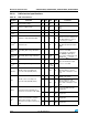
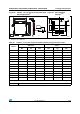
Offset
(3)
Offset error
(difference between measured value
at Code (0x800) and the ideal value =
V
REF+
/2)
±10 mV
Given for the DAC in 12-bit
configuration
±3 LSB
Given for the DAC in 10-bit at
V
REF+
= 3.6 V
±12 LSB
Given for the DAC in 12-bit at
V
REF+
= 3.6 V
Gain
error
(3)
Gain error ±0.5 %
Given for the DAC in 12bit
configuration
t
SETTLING
(
3)
Settling time (full scale: for a 10-bit
input code transition between the
lowest and the highest input codes
when DAC_OUT reaches final value
±1LSB
34 µsC
LOAD
50 pF, R
LOAD
5 k
Update
rate
(3)
Max frequency for a correct
DAC_OUT change when small
variation in the input code (from code i
to i+1LSB)
1MS/sC
LOAD
50 pF, R
LOAD
5 k
t
WAKEUP
(3)
Wakeup time from off state (Setting
the ENx bit in the DAC Control
register)
6.5 10 µs
C
LOAD
50 pF, R
LOAD
5 k
input code between lowest and
highest possible ones.
PSRR+
(1)
Power supply rejection ratio (to V
DDA
)
(static DC measurement
–67 –40 dB No R
LOAD
, C
LOAD
= 50 pF
1. Guaranteed by characterization, not tested in production.
2. Guaranteed by design, not tested in production.
3. Guaranteed by characterization, not tested in production.
Table 46. DAC characteristics (continued)
Symbol Parameter Min Typ Max
(1)
Unit Comments
R
LOAD
C
LOAD
Buffered/Non-buffered DAC
DACx_OUT
Buffer(1)
12-bit
digital to
analog
converter
ai17157