
Datasheet


STM32F100x4, STM32F100x6, STM32F100x8, STM32F100xB Electrical characteristics
Doc ID 16455 Rev 7 69/88
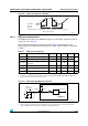
Note: ADC accuracy vs. negative injection current: Injecting a negative current on any analog
input pins should be avoided as this significantly reduces the accuracy of the conversion
being performed on another analog input. It is recommended to add a Schottky diode (pin to
ground) to analog pins which may potentially inject negative currents.
Any positive injection current within the limits specified for I
INJ(PIN)
and I
INJ(PIN)
in
Section 5.3.12 does not affect the ADC accuracy.
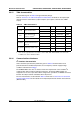
Table 43. R
AIN
max for f
ADC
= 12 MHz
(1)
1. Guaranteed by design, not tested in production.
T
s
(cycles) t
S
(µs) R
AIN
max (k)
1.5 0.125 0.4
7.5 0.625 5.9
13.5 1.125 11.4
28.5 2.375 25.2
41.5 3.45 37.2
55.5 4.625 50
71.5 5.96 NA
239.5 20 NA
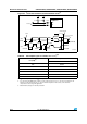
Table 44. ADC accuracy - limited test conditions
(1)(2)
1. ADC DC accuracy values are measured after internal calibration.
2. Based on characterization, not tested in production.
Symbol Parameter Test conditions Typ Max Unit
ET Total unadjusted error f
PCLK2
= 24 MHz,
f
ADC
= 12 MHz, R
AIN
< 10 k,
V
DDA
= 3 V to 3.6 V
V
REF+
= V
DDA
T
A
= 25 °C
Measurements made after
ADC calibration
±1.3 ±2.2
LSB
EO Offset error ±1 ±1.5
EG Gain error ±0.5 ±1.5
ED Differential linearity error ±0.7 ±1
EL Integral linearity error ±0.8 ±1.5
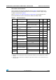
Table 45. ADC accuracy
(1)
(2) (3)
1. ADC DC accuracy values are measured after internal calibration.
2. Better performance could be achieved in restricted V
DD
, frequency, V
REF
and temperature ranges.
3. Based on characterization, not tested in production.
Symbol Parameter Test conditions Typ Max Unit
ET Total unadjusted error
f
PCLK2
= 24 MHz,
f
ADC
= 12 MHz, R
AIN
< 10 k,
V
DDA
= 2.4 V to 3.6 V
T
A
= Full operating range
Measurements made after
ADC calibration
±2 ±5
LSB
EO Offset error ±1.5 ±2.5
EG Gain error ±1.5 ±3
ED Differential linearity error ±1 ±2
EL Integral linearity error ±1.5 ±3