
Datasheet


STM32F100x4, STM32F100x6, STM32F100x8, STM32F100xB Electrical characteristics
Doc ID 16455 Rev 7 67/88
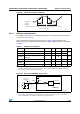
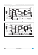
Figure 31. SPI timing diagram - master mode
(1)
1. Measurement points are done at CMOS levels: 0.3V
DD
and 0.7V
DD
.
HDMI consumer electronics control (CEC)
Refer to Section 5.3.12: I/O current injection characteristics for more details on the
input/output alternate function characteristics.
5.3.17 12-bit ADC characteristics
Unless otherwise specified, the parameters given in Ta ble 4 2 are derived from tests
performed under the ambient temperature, f
PCLK2
frequency and V
DDA
supply voltage
conditions summarized in Ta ble 8.
Note: It is recommended to perform a calibration after each power-up.
ai14136
SCK output
CPHA= 0
MOSI
OUTUT
MISO
INP UT
CPHA= 0
MSBIN
M SB OUT
BI T6 IN
LSB OUT
LSB IN
CPOL=0
CPOL=1
B IT1 OUT
NSS input
t
c(SCK)
t
w(SCKH)
t
w(SCKL)
t
r(SCK)
t
f(SCK)
t
h(MI)
High
SCK output
CPHA=1
CPHA=1
CPOL=0
CPOL=1
t
su(MI)
t
v(MO)
t
h(MO)