
Datasheet

STM32F100x4, STM32F100x6, STM32F100x8, STM32F100xB Electrical characteristics
Doc ID 16455 Rev 7 59/88
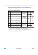
Output voltage levels
Unless otherwise specified, the parameters given in Ta ble 3 5 are derived from tests
performed under the ambient temperature and V
DD
supply voltage conditions summarized
in Ta bl e 8 . All I/Os are CMOS and TTL compliant.
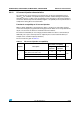
Table 35. Output voltage characteristics
Symbol Parameter Conditions Min Max Unit
V
OL
(1)
1. The I
IO
current sunk by the device must always respect the absolute maximum rating specified in Table 6
and the sum of I
IO
(I/O ports and control pins) must not exceed I
VSS
.
Output Low level voltage for an I/O pin
when 8 pins are sunk at the same time
CMOS port
(2)
I
IO
= +8 mA,
2.7 V < V
DD
< 3.6 V
2. TTL and CMOS outputs are compatible with JEDEC standards JESD36 and JESD52.
0.4
V
V
OH
(3)
3. The I
IO
current sourced by the device must always respect the absolute maximum rating specified in
Table 6 and the sum of I
IO
(I/O ports and control pins) must not exceed I
VDD
.
Output High level voltage for an I/O pin
when 8 pins are sourced at the same time
V
DD
–0.4
V
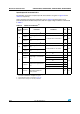
OL
(1)
Output low level voltage for an I/O pin
when 8 pins are sunk at the same time
TTL port
(2)
I
IO
= +8 mA
2.7 V < V
DD
< 3.6 V
0.4
V
V
OH
(3)
Output high level voltage for an I/O pin
when 8 pins are sourced at the same time
2.4
V
OL
(1)
Output low level voltage for an I/O pin
when 8 pins are sunk at the same time
I
IO
= +20 mA
(4)
2.7 V < V
DD
< 3.6 V
4. Based on characterization data, not tested in production.
1.3
V
V
OH
(3)
Output high level voltage for an I/O pin
when 8 pins are sourced at the same time
V
DD
–1.3
V
OL
(1)
Output low level voltage for an I/O pin
when 8 pins are sunk at the same time
I
IO
= +6 mA
(4)
2 V < V
DD
< 2.7 V
0.4
V
V
OH
(3)
Output high level voltage for an I/O pin
when 8 pins are sourced at the same time
V
DD
–0.4