
Datasheet

Electrical characteristics STM32F100x4, STM32F100x6, STM32F100x8, STM32F100xB
58/88 Doc ID 16455 Rev 7
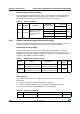
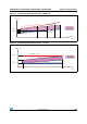
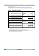
Figure 24. 5 V tolerant I/O input characteristics - CMOS port
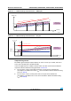
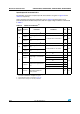
Figure 25. 5 V tolerant I/O input characteristics - TTL port
Output driving current
The GPIOs (general-purpose inputs/outputs) can sink or source up to ±8 mA, and sink or
source up to ±20 mA (with a relaxed V
OL
/V
OH
).
In the user application, the number of I/O pins which can drive current must be limited to
respect the absolute maximum rating specified in Section 5.2:
● The sum of the currents sourced by all the I/Os on V
DD,
plus the maximum Run
consumption of the MCU sourced on V
DD,
cannot exceed the absolute maximum rating
I
VDD
(see Ta ble 6).
● The sum of the currents sunk by all the I/Os on V
SS
plus the maximum Run
consumption of the MCU sunk on V
SS
cannot exceed the absolute maximum rating
I
VSS
(see Ta bl e 6 ).
6$$
#-/3STANDARDREQUIREMENTS6
)(
6
$$
#-/3STANDARDREQUIRMENT6
),
6
$$
6
)(
6
),
6
6
$$
6
)NPUTRANGE
NOTGUARANTEED
AIB
6
)(
6
$$
6
),
6
$$
NOTGUARANTEED
)NPUTRANGE
44,REQUIREMENT6
)(
6
6
)(
6
$$
6
),
6
$$
44,REQUIREMENTS6
),
6
6
)(
6
),
6
6
$$
6
7
),MAX
7
)(MIN
AI