
Datasheet

STM32F100x4, STM32F100x6, STM32F100x8, STM32F100xB Electrical characteristics
Doc ID 16455 Rev 7 45/88
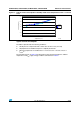
Low-speed external user clock generated from an external source
The characteristics given in Tab l e 2 0 result from tests performed using an low-speed
external clock source, and under the ambient temperature and supply voltage conditions
summarized in Table 8.
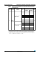
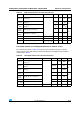
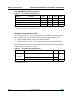
Table 19. High-speed external user clock characteristics
Symbol Parameter Conditions Min Typ Max Unit
f
HSE_ext
User external clock source
frequency
(1)
1. Guaranteed by design, not tested in production.
1824MHz
V
HSEH
OSC_IN input pin high level
voltage
(1)
0.7V
DD
V
DD
V
V
HSEL
OSC_IN input pin low level
voltage
(1)
V
SS
0.3V
DD
t
w(HSE)
t
w(HSE)
OSC_IN high or low time
(1)
5
ns
t
r(HSE)
t
f(HSE)
OSC_IN rise or fall time
(1)
20
C
in(HSE)
OSC_IN input capacitance
(1)
5pF
DuCy
(HSE)
Duty cycle
(1)
45 55 %
I
L
OSC_IN Input leakage current V
SS
V
IN
V
DD
±1 µA
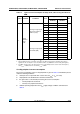
Table 20. Low-speed external user clock characteristics
Symbol Parameter Conditions Min Typ Max Unit
f
LSE_ext
User external clock source
frequency
(1)
1. Guaranteed by design, not tested in production.
32.768 1000 kHz
V
LSEH
OSC32_IN input pin high level
voltage
(1)
0.7V
DD
V
DD
V
V
LSEL
OSC32_IN input pin low level
voltage
(1)
V
SS
0.3V
DD
t
w(LSE)
t
w(LSE)
OSC32_IN high or low time
(1)
450
ns
t
r(LSE)
t
f(LSE)
OSC32_IN rise or fall time
(1)
50
C
in(LSE)
OSC32_IN input capacitance
(1)
5pF
DuCy
(LSE)
Duty cycle
(1)
30 70 %
I
L
OSC32_IN Input leakage current V
SS
V
IN
V
DD
±1 µA