
Datasheet


Electrical characteristics STM32F100x4, STM32F100x6, STM32F100x8, STM32F100xB
68/88 Doc ID 16455 Rev 7
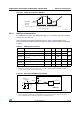
Equation 1: R
AIN
max formula:
The above formula (Equation 1) is used to determine the maximum external impedance allowed for an
error below 1/4 of LSB. Here N = 12 (from 12-bit resolution).
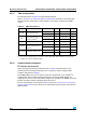
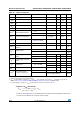
Table 42. ADC characteristics
Symbol Parameter Conditions Min Typ
Max Unit
V
DDA
Power supply 2.4 3.6 V
V
REF+
Positive reference voltage 2.4 V
DDA
V
I
VREF
Current on the V
REF
input
pin
160
(1)
220
(1)
µA
f
ADC
ADC clock frequency 0.6 12 MHz
f
S
(2)
Sampling rate 0.05 1 MHz
f
TRIG
(2)
External trigger frequency
f
ADC
= 12 MHz 823 kHz
17 1/f
ADC
V
AIN
(3)
Conversion voltage range
0 (V
SSA
tied to
ground)
V
REF+
V
R
AIN
(2)
External input impedance
See Equation 1 and
Ta bl e 4 3 for details
50 k
R
ADC
(2)
Sampling switch resistance 1 k
C
ADC
(2)
Internal sample and hold
capacitor
8pF
t
CAL
(2)
Calibration time
f
ADC
= 12 MHz 5.9 µs
83 1/f
ADC
t
lat
(2)
Injection trigger conversion
latency
f
ADC
= 12 MHz 0.214 µs
3
(4)
1/f
ADC
t
latr
(2)
Regular trigger conversion
latency
f
ADC
= 12 MHz 0.143 µs
2
(4)
1/f
ADC
t
S
(2)
Sampling time f
ADC
= 12 MHz
0.125 17.1 µs
1.5 239.5 1/f
ADC
t
STAB
(2)
Power-up time 0 0 1 µs
t
CONV
(2)
Total conversion time
(including sampling time)
f
ADC
= 12 MHz 1.17 21 µs
14 to 252 (t
S
for sampling +12.5 for
successive approximation)
1/f
ADC
1. Based on characterization results, not tested in production.
2. Guaranteed by design, not tested in production.
3. V
REF+
can be internally connected to V
DDA
and V
REF-
can be internally connected to V
SSA
, depending on the package.
Refer to Table 4: Low & medium-density STM32F100xx pin definitions and Figure 6 for further details.
4. For external triggers, a delay of 1/f
PCLK2
must be added to the latency specified in Table 42.
R
AIN
T
S
f
ADC
C
ADC
2
N2+
ln
------------------------------------------------------------- - R
ADC
–