
Datasheet

Electrical characteristics STM32F100x4, STM32F100x6, STM32F100x8, STM32F100xB
56/88 Doc ID 16455 Rev 7
5.3.13 I/O port characteristics
General input/output characteristics
Unless otherwise specified, the parameters given in Ta ble 3 4 are derived from tests
performed under the conditions summarized in Tabl e 8 . All I/Os are CMOS and TTL
compliant.
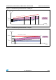
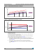
All I/Os are CMOS and TTL compliant (no software configuration required). Their
characteristics cover more than the strict CMOS-technology or TTL parameters. The
coverage of these requirements is shown in Figure 22 and Figure 23 for standard I/Os, and
in Figure 24 and Figure 25 for 5 V tolerant I/Os.
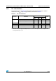
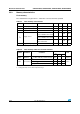
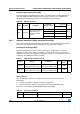
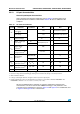
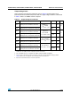
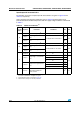
Table 34. I/O static characteristics
Symbol Parameter Conditions Min Typ
Max Unit
V
IL
Standard I/O input low
level voltage
–0.3 0.28*(V
DD
–2 V)+0.8 V
V
I/O FT
(1)
input low
level voltage
–0.3 0.32*(V
DD
–2 V)+0.75 V
V
IH
Standard I/O input
high level voltage
0.41*(V
DD
–2 V) +1.3 V V
DD
+0.3
I/O FT
(1)
input high
level voltage
V
DD
2 V
0.42*(V
DD
–2)+1 V
5.5
V
DD
2 V 5.2
V
hys
Standard I/O Schmitt
trigger voltage
hysteresis
(2)
200 mV
I/O FT Schmitt trigger
voltage hysteresis
(2)
5% V
DD
(3)
mV
I
lkg
Input leakage
current
(4)
V
SS
V
IN
V
DD
Standard I/Os
1
µA
V
IN
= 5 V
I/O FT
3
R
PU
Weak pull-up
equivalent resistor
(5)
V
IN
V
SS
30 40 50 k
R
PD
Weak pull-down
equivalent resistor
(5)
V
IN
V
DD
30 40 50 k
C
IO
I/O pin capacitance 5 pF
1. FT = 5V tolerant. To sustain a voltage higher than V
DD
+0.3 the internal pull-up/pull-down resistors must be disabled.
2. Hysteresis voltage between Schmitt trigger switching levels. Guaranteed by design, not tested in production.
3. With a minimum of 100 mV.
4. Leakage could be higher than max. if negative current is injected on adjacent pins.
5. Pull-up and pull-down resistors are designed with a true resistance in series with a switchable PMOS/NMOS. This
PMOS/NMOS contribution
to the series resistance is minimum (~10% order).