
Datasheet


STM32F051x Electrical characteristics
Doc ID 022265 Rev 3 91/105
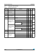
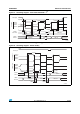
Figure 29. I2S slave timing diagram (Philips protocol)
1. Measurement points are done at CMOS levels: 0.3 × VDD and 0.7 × VDD.
2. LSB transmit/receive of the previously transmitted byte. No LSB transmit/receive is sent before the first
byte.
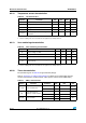
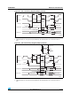
Figure 30. I2S master timing diagram (Philips protocol)
1. Data based on characterization results, not tested in production.
2. LSB transmit/receive of the previously transmitted byte. No LSB transmit/receive is sent before the first
byte.
CK Input
CPOL = 0
CPOL = 1
t
c(CK)
WS input
SD
transmit
SD
receive
t
w(CKH)
t
w(CKL)
t
su(WS)
t
v(SD_ST)
t
h(SD_ST)
t
h(WS)
t
su(SD_SR)
t
h(SD_SR)
MSB receive Bitn receive LSB receive
MSB transmit Bitn transmit LSB transmit
ai14881b
LSB receive
(2)
LSB transmit
(2)
CK output
CPOL = 0
CPOL = 1
t
c(CK)
WS output
SD
receive
SD
transmit
t
w(CKH)
t
w(CKL)
t
su(SD_MR)
t
v(SD_MT)
t
h(SD_MT)
t
h(WS)
t
h(SD_MR)
MSB receive Bitn receive LSB receive
MSB transmit Bitn transmit LSB transmit
ai14884b
t
f(CK)
t
r(CK)
t
v(WS)
LSB receive
(2)
LSB transmit
(2)