
Datasheet


Electrical characteristics STM32F051x
78/105 Doc ID 022265 Rev 3
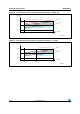
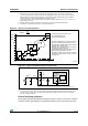
Equation 1: R
AIN
max formula
The formula above (Equation 1) is used to determine the maximum external impedance
allowed for an error below 1/4 of LSB. Here N = 12 (from 12-bit resolution).
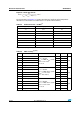
Table 55. R
AIN
max for f
ADC
= 14 MHz
(1)
1. Guaranteed by design, not tested in production.
T
s
(cycles) t
S
(µs) R
AIN
max (kΩ)
1.5 0.11 0.4
7.5 0.54 5.9
13.5 0.96 11.4
28.5 2.04 25.2
41.5 2.96 37.2
55.5 3.96 50
71.5 5.11 NA
239.5 17.1 NA
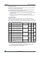
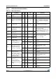
Table 56. ADC accuracy
(1)(2) (3)
1. ADC DC accuracy values are measured after internal calibration.
Symbol Parameter Test conditions Typ Max
(4)
Unit
ET Total unadjusted error
f
PCLK
= 48 MHz,
f
ADC
= 14 MHz, R
AIN
< 10 kΩ,
V
DDA
= 3 V to 3.6 V
T
A
= 25 °C
±1.3 ±2
LSB
EO Offset error ±1 ±1.5
EG Gain error ±0.5 ±1.5
ED Differential linearity error ±0.7 ±1
EL Integral linearity error ±0.8 ±1.5
ET Total unadjusted error
f
PCLK
= 48 MHz,
f
ADC
= 14 MHz, R
AIN
< 10 kΩ,
V
DDA
= 2.7 V to 3.6 V
T
A
= −40 to 105 °C
±3.3 ±4
LSB
EO Offset error ±1.9 ±2.8
EG Gain error ±2.8 ±3
ED Differential linearity error ±0.7 ±1.3
EL Integral linearity error ±1.2 ±1.7
ET Total unadjusted error
f
PCLK
= 48 MHz,
f
ADC
= 14 MHz, R
AIN
< 10 kΩ,
V
DDA
= 2.4 V to 3.6 V
T
A
= 25 °C
±3.3 ±4
LSB
EO Offset error ±1.9 ±2.8
EG Gain error ±2.8 ±3
ED Differential linearity error ±0.7 ±1.3
EL Integral linearity error ±1.2 ±1.7
R
AIN
T
S
f
ADC
C
ADC
2
N2+
()ln××
-------------------------------------------------------------- R
ADC
–<