
Datasheet


STM32F051x Electrical characteristics
Doc ID 022265 Rev 3 77/105
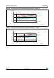
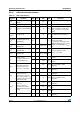
6.3.15 12-bit ADC characteristics
Unless otherwise specified, the parameters given in Ta ble 5 4 are preliminary values derived
from tests performed under ambient temperature, f
PCLK2
frequency and V
DDA
supply voltage
conditions summarized in Ta bl e 2 0.
Note: It is recommended to perform a calibration after each power-up.
Table 54. ADC characteristics
Symbol Parameter Conditions Min Typ
Max Unit
V
DDA
Analog supply voltage for
ADC ON
2.4 - 3.6 V
f
ADC
ADC clock frequency 0.6 - 14 MHz
f
S
(1)
Sampling rate 0.05 - 1 MHz
f
TRIG
(1)
External trigger frequency
f
ADC
= 14 MHz - - 823 kHz
--171/f
ADC
V
AIN
Conversion voltage range 0 - V
DDA
V
R
AIN
(1)
External input impedance
See Equation 1 and
Tabl e 5 5 for details
--50kΩ
R
ADC
(1)
Sampling switch resistance - - 1 kΩ
C
ADC
(1)
Internal sample and hold
capacitor
--8pF
t
CAL
(1)
Calibration time
f
ADC
= 14 MHz 5.9 µs
83 1/f
ADC
t
latr
(1)
Trigger conversion latency
f
ADC
= f
PCLK
/2 = 14 MHz 0.196 µs
f
ADC
= f
PCLK
/2 5.5 1/f
PCLK
f
ADC
= f
PCLK
/4 = 12 MHz 0.219 µs
f
ADC
= f
PCLK
/4 10.5 1/f
PCLK
f
ADC
= f
HSI14
= 14 MHz 0.188 - 0.259 µs
Jitter
ADC
ADC jitter on trigger
conversion
f
ADC
= f
HSI14
-1-1/f
HSI14
t
S
(1)
Sampling time
f
ADC
= 14 MHz 0.107 - 17.1 µs
1.5 - 239.5 1/f
ADC
t
STAB
(1)
Power-up time 0 0 1 µs
t
CONV
(1)
Total conversion time
(including sampling time)
f
ADC
= 14 MHz 1 18 µs
14 to 252 (t
S
for sampling +12.5 for
successive approximation)
1/f
ADC
1. Guaranteed by design, not tested in production.