
Datasheet


Electrical characteristics STM32F051x
76/105 Doc ID 022265 Rev 3
6.3.14 NRST pin characteristics
The NRST pin input driver uses CMOS technology. It is connected to a permanent pull-up
resistor, R
PU
(see Ta ble 5 0 ).
Unless otherwise specified, the parameters given in Ta bl e 5 3 are derived from tests
performed under ambient temperature and VDD supply voltage conditions summarized in
Table 2 0 .
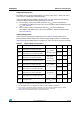
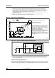
Figure 21. Recommended NRST pin protection
1. The reset network protects the device against parasitic resets.
2. The user must ensure that the level on the NRST pin can go below the V
IL(NRST)
max level specified in
Table 53. Otherwise the reset will not be taken into account by the device.
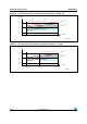
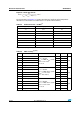
Table 53. NRST pin characteristics
Symbol Parameter Conditions Min Typ Max Unit
V
IL(NRST)
(1)
1. Guaranteed by design, not tested in production.
NRST Input low level voltage –0.3 - 0.8
V
V
IH(NRST)
(1)
NRST Input high level voltage 2 - V
DD
+0.3
V
hys(NRST)
NRST Schmitt trigger voltage
hysteresis
- 200 - mV
R
PU
Weak pull-up equivalent resistor
(2)
2. The pull-up is designed with a true resistance in series with a switchable PMOS. This PMOS contribution
to the series resistance must be minimum (~10% order).
V
IN
= V
SS
30 40 50 kΩ
V
F(NRST)
(1)
NRST Input filtered pulse - - 100 ns
V
NF(NRST)
(1)
NRST Input not filtered pulse 300 - - ns
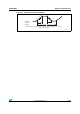
-36
2
05
.234
6
$$
&ILTER
)NTERNAL2ESET
&
%XTERNAL
RESETCIRCUIT