
Datasheet


STM32F051x Electrical characteristics
Doc ID 022265 Rev 3 41/105
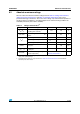
6.2 Absolute maximum ratings
Stresses above the absolute maximum ratings listed in Table 17: Voltage characteristics,
Table 18: Current characteristics, and Table 19: Thermal characteristics may cause
permanent damage to the device. These are stress ratings only and functional operation of
the device at these conditions is not implied. Exposure to maximum rating conditions for
extended periods may affect device reliability.
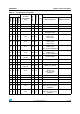
Table 17. Voltage characteristics
(1)
1. All main power (V
DD
, V
DDA
) and ground (V
SS
, V
SSA
) pins must always be connected to the external power
supply, in the permitted range.
Symbol Ratings Min Max Unit
V
DD
–V
SS
External main supply voltage
(including V
DDA
and V
DD
)
–0.3 4.0 V
V
DD
–V
DDA
Allowed voltage difference for V
DD
> V
DDA
-0.4V
V
IN
(2)
2. V
IN
maximum must always be respected. Refer to Table 18: Current characteristics for the maximum
allowed injected current values.
Input voltage on FT and FTf pins V
SS
− 0.3 V
DD
+ 4.0 V
Input voltage on TTa pins V
SS
− 0.3 4.0 V
Input voltage on any other pin V
SS
− 0.3 4.0 V
|ΔV
DDx
|
Variations between different V
DD
power pins
-50mV
|V
SSX
− V
SS
|
Variations between all the different
ground pins
-50mV
V
ESD(HBM)
Electrostatic discharge voltage
(human body model)
see Section 6.3.11: Electrical
sensitivity characteristics