
Datasheet


STM32F050xx Electrical characteristics
Doc ID 023683 Rev 1 79/97
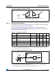
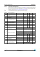
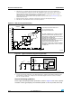
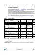
Table 59. SPI characteristics
Symbol Parameter Conditions Min Max Unit
f
SCK
1/t
c(SCK)
SPI clock frequency
Master mode - 18
MHz
Slave mode - 18
t
r(SCK)
t
f(SCK)
SPI clock rise and fall
time
Capacitive load: C = 15 pF - 6 ns
t
su(NSS)
(1)
NSS setup time Slave mode 4Tpclk -
ns
t
h(NSS)
(1)
NSS hold time Slave mode 2Tpclk + 10 -
t
w(SCKH)
(1)
t
w(SCKL)
(1)
SCK high and low time
Master mode, f
PCLK
= 36 MHz,
presc = 4
Tpclk/2 -2 Tpclk/2 + 1
t
su(MI)
(1)
t
su(SI)
(1)
Data input setup time
Master mode 4 -
Slave mode 5 -
t
h(MI)
(1)
Data input hold time
Master mode 4 -
t
h(SI)
(1)
Slave mode 5 -
t
a(SO)
(1)(2)
Data output access time Slave mode, f
PCLK
= 20 MHz 0 3Tpclk
t
dis(SO)
(1)(3)
Data output disable time Slave mode 0 18
t
v(SO)
(1)
Data output valid time Slave mode (after enable edge) - 22.5
t
v(MO)
(1)
Data output valid time Master mode (after enable edge) - 6
t
h(SO)
(1)
Data output hold time
Slave mode (after enable edge) 11.5 -
t
h(MO)
(1)
Master mode (after enable edge) 2 -
DuCy(SCK)
SPI slave input clock duty
cycle
Slave mode 25 75 %
1. Data based on characterization results, not tested in production.
2. Min time is for the minimum time to drive the output and the max time is for the maximum time to validate the data.
3. Min time is for the minimum time to invalidate the output and the max time is for the maximum time to put the data in Hi-Z