
Datasheet


STM32F050xx Electrical characteristics
Doc ID 023683 Rev 1 59/97
Low-speed internal (LSI) RC oscillator
Wakeup time from low-power mode
The wakeup times given in Table 3 6 is measured on a wakeup phase with a 8-MHz HSI RC
oscillator. The event used to wake up the device depends from the current operating mode:
● Stop or sleep mode: the wakeup event is WFE.
● The wakeup pin used in sleep, stop and standby modes is PA0.
All timings are derived from tests performed under ambient temperature and V
DD
supply
voltage conditions summarized in Table 15: General operating conditions.
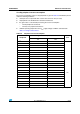
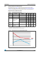
Table 35. LSI oscillator characteristics
(1)
1.
V
DDA
= 3.3 V, T
A
= –40 to 105 °C unless otherwise specified.
Symbol Parameter Min Typ Max Unit
f
LSI
Frequency 30 40 50 kHz
t
su(LSI)
(2)
2. Guaranteed by design, not tested in production.
LSI oscillator startup time - - 85 µs
I
DDA(LSI)
(2)
LSI oscillator power consumption - 0.75 1.2 µA
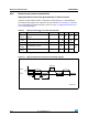
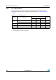
Table 36. Low-power mode wakeup timings
Symbol Parameter Conditions
Typ @VDD
Max Unit
= 2.0 V = 2.4 V = 2.7 V = 3 V = 3.3 V
t
WUSTOP
Wakeup from Stop
mode
Regulator in run
mode
4.24.24.24.24.25
µs
Regulator in low
power mode
8.05 7.05 6.6 6.27 6.05 9
t
WUSTANDBY
Wakeup from
Standby mode
60.35 55.6 53.5 52.02 50.96
t
WUSLEEP
Wakeup from Sleep
mode
1.11.11.11.11.1