
Datasheet


Electrical characteristics STM32F050xx
38/97 Doc ID 023683 Rev 1
2. This current consumption must be correctly distributed over all I/Os and control pins. The total output current must not be
sunk/sourced between two consecutive power supply pins referring to high pin count QFP packages.
3. Positive injection is not possible on these I/Os and does not occur for input voltages lower than the specified maximum
value.
4. A positive injection is induced by V
IN
>V
DD
while a negative injection is induced by V
IN
<V
SS
. I
INJ(PIN)
must never be
exceeded. Refer to Table 12: Voltage characteristics for the maximum allowed input voltage values.
5. A positive injection is induced by V
IN
>V
DDA
while a negative injection is induced by V
IN
<V
SS
. I
INJ
(PIN) must never be
exceeded. Refer also to Table 12: Voltage characteristics for the maximum allowed input voltage values. Negative injection
disturbs the analog performance of the device. See note
(2)
below Table 51: ADC accuracy.
6. When several inputs are submitted to a current injection, the maximum ΣI
INJ(PIN)
is the absolute sum of the positive and
negative injected currents (instantaneous values).
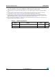
Table 14. Thermal characteristics
Symbol Ratings Value Unit
T
STG
Storage temperature range –65 to +150 °C
T
J
Maximum junction temperature 150 °C