
Datasheet


STM32F050xx Electrical characteristics
Doc ID 023683 Rev 1 41/97
6.3.4 Embedded reference voltage
The parameters given in Ta bl e 1 9 are derived from tests performed under ambient
temperature and V
DD
supply voltage conditions summarized in Table 15: General operating
conditions.
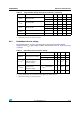
V
PVD5
PVD threshold 5
Rising edge 2.57 2.68 2.79 V
Falling edge 2.47 2.58 2.69 V
V
PVD6
PVD threshold 6
Rising edge 2.66 2.78 2.9 V
Falling edge 2.56 2.68 2.8 V
V
PVD7
PVD threshold 7
Rising edge 2.76 2.88 3 V
Falling edge 2.66 2.78 2.9 V
V
PVDhyst
(2)
PVD hysteresis - 100 - mV
I
DD(PVD)
PVD current consumption - 0.15 0.26 µA
1. Data based on characterization results only, not tested in production.
2. Guaranteed by design, not tested in production.
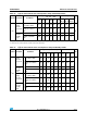
Table 18. Programmable voltage detector characteristics (continued)
Symbol Parameter Conditions Min
(1)
Typ Max
(1)
Unit
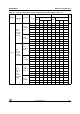
Table 19. Embedded internal reference voltage
Symbol Parameter Conditions Min Typ Max Unit
V
REFINT
Internal reference voltage
–40 °C < T
A
< +105 °C 1.16 1.2 1.25 V
–40 °C < T
A
< +85 °C 1.16 1.2 1.24
(1)
1. Data based on characterization results, not tested in production.
V
T
S_vrefint
(2)
2. Shortest sampling time can be determined in the application by multiple iterations.
ADC sampling time when
reading the internal
reference voltage
- 5.1 17.1
(3)
3. Guaranteed by design, not tested in production.
µs
ΔV
REFINT
Internal reference voltage
spread over the
temperature range
V
DDA
= 3 V ±10 mV - -
10
(3)
mV
T
Coeff
Temperature coefficient - -
100
(3)
ppm/°C